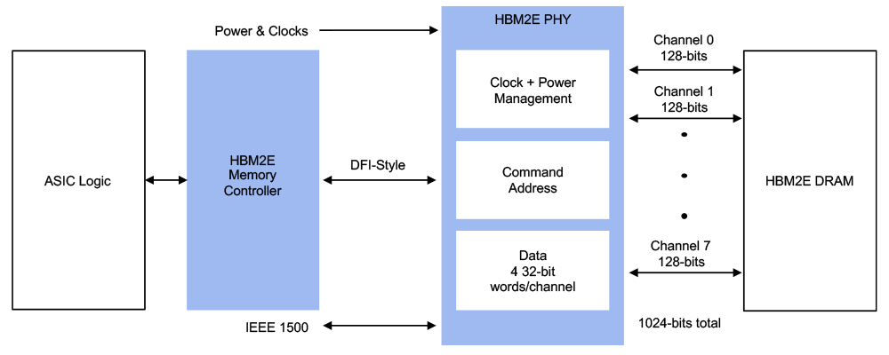
HBM 是一款高性能内存,特点是功耗低、尺寸小。它以更低的时钟速度(与 DDR4 相比)将 2.5D 封装与更宽的接口相结合,从而以更高的带宽功耗比效率为高性能计算应用提供更高的总吞吐量。
Rambus HBM Gen2 PHY 完全符合 JEDEC HBM2 标准,支持每个数据引脚高达 2000 Mbps 的数据速率,总带宽因此达到 256 GB/s。该接口具有 8 个独立信道,每个信道包含 128 位,总数据宽度为 1024 位,支持 2、4 或 8 个 DRAM 的堆栈高度。此外,PHY 专为 2.5D 系统设计,配有在 DRAM 和 PHY 之间路由信号的内插器。这种信号密度和堆叠式外形的结合需要考虑特殊的设计。为了在这种复杂的系统中便于实现并提高设计的灵活性,Rambus 对整个 2.5D 系统进行完整的信号与电源完整性分析,以确保满足所有信号、功耗和散热要求。
The HBM2E controller supports both HBM2 and HBM2E devices with data rates of up to 3.6 Gbps per data pin. It supports all standard channel densities including 4, 6, 8, 12, 16 and 24 Gb. The controller maximizes memory bandwidth and minimizes latency via Look-Ahead command processing. The core is DFI compatible (with extensions added for HBM2E) and supports AXI, OCP or native interface to user logic.
The Rambus HBM2E PHY and HBM2E controller used together comprise a complete HBM2E memory interface subsystem. Alternatively, these cores can be licensed separately to be paired with 3rd-party HBM2E controller or PHY solutions.
全面的芯片和系统设计审查
工程设计服务:
For AI and HPC applications, HBM2E memory can deliver excellent bandwidth, capacity and latency in a very compact footprint thanks to its 2.5D/3D structure. The flipside is that this same structure leads to greater design complexity and raises a new set of implementation considerations.
| 协议 | 数据速率 (Gbps) | 应用 |
|---|---|---|
| HBM2 | 0.5-2000 | 数据中心和网络 |
News
Related Papers
Webinars