Traditional, multi-gigahertz memory interfaces require timing synchronization circuitry in both the controller and memory interface in order to compensate for any skew that arises between clock, data, and command/address (C/A) signals. FlexClocking™ Architecture technology is an architecture that utilizes asymmetric partitioning and places critical calibration and timing circuitry in the controller interface, greatly simplifying the design of the DRAM interface. The clock is forwarded and distributed to both the controller circuit blocks and the DRAM device from a central PLL located in the memory controller interface (PHY).
- Reduces DRAM power consumption
- Simplifies DRAM interface design
- Enables fast power state transition times
- Eliminates PLL or DLL on DRAM
What is FlexClocking Architecture Technology?
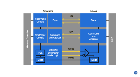
This architecture features the use of a single clock multiplier where the DRAM interface operates in a single, high-speed clock domain derived from a half-bit-rate clock forwarded from the controller. The command/address (C/A) and data (DQ) links are implemented as bi-directional differential serial transceivers with 8:1 multiplexing. A peak interface bandwidth of greater than 17GB/s can be achieved using only four bytes of DQ links operating at 4.3Gbps, 8 C/A links, and a single forwarded clock operating at 2.15GHz.
Given this unique topology, the FlexClocking™ Architecture enables high-speed operation without the need for a DLL or PLL on the DRAM device. This is made possible in part by the Rambus FlexPhase™ technology which is used to adjust for any variability between the clock and DQ signals received at the DRAM device. As a result, DRAM design is simplified and power consumption is significantly reduced.
Who Benefits?
FlexClocking™ Architecture enables high-speed operation in a memory system without the need for a PLL and/or DLL on the DRAM, reducing complexity and cost for DRAM designers. In addition, it allows for fast transition times from low-power to active modes and superior power efficiency delivering enhance response times and increased battery life to end users.