• Skip to primary navigation
  • Skip to main content
  • Skip to footer
  • English
  • Investor Relations
  • Resource Library
  • Newsroom
  • Blog
  • Careers
  • Support Center
Rambus Logo

Rambus

At Rambus, we create cutting-edge semiconductor and IP products, spanning memory and interfaces to security, smart sensors and lighting.

  • Products
      • All
          • Memory Interface Chips
          • DIMM Chipsets
          • DDR5 DIMM Chipset
          • DDR4 NVRCD
          • DDR4 Register Clock Driver
          • DDR4 Data Buffer
          • CXL Memory Interconnect Initiative
          • Interface IP
          • Memory PHYs
          • GDDR6 PHY
          • HBM3 PHY
          • HBM2E PHY
          • DDR4 PHY
          • More…
          • SerDes PHYs
          • PCIe 6.0 PHY
          • PCIe 5.0 PHY
          • 32G C2C PHY
          • 32G PHY
          • 28G PHY
          • More…
          • Digital Controllers
          • Memory Controllers
          • CXL & PCI Express Controllers
          • MIPI Controllers
          • Video Compression and Forward Error Correction Cores
          • Security IP
          • Root of Trust Solutions
          • Security Protocol Engines
          • Inline Cipher Engines
          • Crypto Accelerator Cores
          • DPA Countermeasures
          • Software Protocols & Crypto Toolkits
          • Anti-Counterfeiting
          • Provisioning and Key Management
      • Memory Interface Chips
        • DIMM Chipsets
          • DDR5 DIMM Chipset
          • Non-Volatile DDR4 Registering Clock Driver
          • DDR4 Register Clock Driver
          • DDR4 Data Buffer
          • DDR3 Register Clock Driver
          • DDR3 Isolation Memory Buffer
        • CXL Memory Interconnect Initiative

        • Made for high speed, reliability and power efficiency, our DDR3, DDR4, and DDR5 DIMM chipsets deliver top-of-the-line performance and capacity for the next wave of computing systems. Learn more about our Memory Interface Chip solutions
      • Interface IP
          • Memory PHYs
            • GDDR6 PHY
            • HBM3 PHY
            • HBM2E PHY
            • DDR4 PHY
            • DDR4 Multi-modal PHY
            • DDR3 PHY
          • SerDes PHYs
            • PCIe 6.0 PHY
            • PCIe 5.0 PHY
            • PCIe 4.0 PHY
            • 32G C2C PHY
            • 32G PHY
            • 28G PHY
            • 16G PHY
            • 12G PHY
            • 6G PHY
          • Digital Controllers
            • HBM3 Controller
            • HBM2E Controller
            • GDDR6 Controller
            • LPDDR5 Controller
            • CXL 2.0 Controller
            • PCIe 6.0 Controller
            • PCIe 5.0 Controller
            • MIPI CSI-2/DSI-2 Controllers
            • Video Compression and Forward Error Correction Cores
            • More…

        • With their reduced power consumption and industry-leading data rates, our line-up of memory interface IP solutions support a broad range of industry standards with improved margin and flexibility. Learn more about our Interface IP solutions
      • Security IP
          • Root of Trust Solutions
          • Security Protocol Engines
            • MACsec Engines
            • IPsec, TLS, SSL Multi-Protocol Engines
            • High Speed Public Key Accelerator
          • Inline Cipher Engines
          • Crypto Accelerator Cores
            • DPA Resistant Cores
            • Basic Crypto Blocks
          • Anti-Counterfeiting
            • CryptoFirewall Cores
            • Circuit Camouflage Technology
          • DPA Countermeasures
            • DPA Resistant Cores
            • DPA Resistant Software Libraries
            • DPA Workstation Platform
          • Software Protocols & Crypto Toolkits
            • IPsec Toolkit
            • FIPs Cryptographic Libraries
            • MACsec Toolkit
            • IoT Security Framework
          • CryptoMedia
            • Content Protection Core
            • Content Protection Services
          • Provisioning and Key Management
            • CryptoManager Provisioning
            • CryptoManager Device Key Management

        • From chip-to-cloud-to-crowd, Rambus secure silicon IP helps protect the world’s most valuable resource: data. Securing electronic systems at their hardware foundation, our embedded security solutions span areas including root of trust, tamper resistance, content protection and trusted provisioning. Learn more about our Security IP offerings
  • Markets
      • AI & Machine Learning
        • Speed and Security for the Artificial Intelligence & Machine Learning Revolution
          • Products
          • SerDes PHYs
          • Memory PHYs
          • Digital Controllers
          • Memory Interface Chips
          • Root of Trust
          • Crypto Accelerator Cores
          • Protocol Engines
          • Provisioning and Key Management
          • AI & Machine Learning
      • Automotive
        • Providing Performance & Security for the Connected Car
          • Products
          • Memory PHYs
          • SerDes PHYs
          • Digital Controllers
          • Root of Trust
          • PKE Engine
          • MACsec Engines
          • Crypto Accelerator Cores
          • Provisioning and Key Management
          • Explore Automotive
      • Data Center
        • Optimizing capacity, connectivity and capability of the cloud
          • Products
          • SerDes PHYs
          • Memory PHYs
          • Digital Controllers
          • Memory Interface Chips
          • Root of Trust
          • MACsec Engines
          • Software Protocols
          • Provisioning and Key Management
          • See Data Center
      • Edge
        • Catching a tidal wave of data
          • Products
          • Memory PHYs
          • SerDes PHYs
          • Digital Controllers
          • Root of Trust
          • Crypto Accelerator Cores
          • Protocol Engines
          • Software Protocols
          • Discover Edge
      • Government
        • Securing Mission-critical Systems
          • Products
          • Root of Trust
          • Protocol Engines
          • Anti-Tamper Cores
          • Provisioning and Key Management
          • DPA Workstation Platform
          • SerDes PHYs
          • Memory PHYs
          • Digital Controllers
          • See Government
      • IoT
        • Making IoT Data Safe & Fast
          • Products
          • Root of Trust
          • TLS Toolkits
          • Provisioning and Key Management
          • Memory PHYs
          • SerDes PHYs
          • Digital Controllers
          • Explore IoT
  • Resources
    • Inventions
    • Buying Guide
    • Resource Library
      • Webinars
      • Product Selector
  • About
      • Corporate Overview
      • Leadership
      • Inventors
      • Careers
      • Locations
      • Investor Relations
      • Newsroom
      • Blog
      • Events
      • Partnerships
      • Certifications
      • Corporate Responsibility
      • Contact
Home > Inventions > Memory + Interfaces

Memory + Interfaces

Phase Interpolator-Based CDR

In order to communicate data from one chip to another across a signal line, the receiving chip must know when to sample the data signal that it receives from the transmitting chip. In many systems, this information is provided by a timing (clock) signal sent from the transmitting chip to the receiving chip along a dedicated timing signal line adjacent to the data signal line. In systems with higher signaling rates, the receiving chip typically requires a clock alignment circuit, such as a Phase Locked Loop (PLL) or Delay Locked Loop (DLL), but the data timing must still be well-matched in order to eliminate timing skews. A phase interpolator based clock-data recovery circuit (CDR) is an alternative circuit architecture developed by Rambus which provides multiple advantages compared to PLL-based CDRs.

  • Reduces cost, power and area of a CDR
  • Improves jitter performance in high-speed links

What is Phase Interpolator-Based CDR Technology?

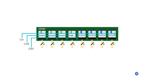
Buffered modules introduce a memory buffer between the memory controller and the DRAM devices on each module, isolating the DRAM from the memory bus and enabling an increase to the width of the memory without increasing the pin count of the controller. This also reduces the effective capacitive load on the memory bus enabling support for multiple modules at high speed.
Phase interpolator-based clock and data recovery

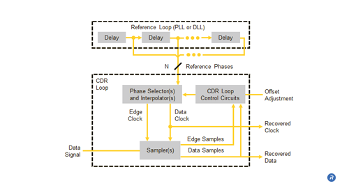
A phase-interpolator based CDR is an alternative circuit architecture developed by Rambus which provides multiple advantages compared to PLL-based CDRs. This type of CDR uses a PLL or DLL to implement a reference loop which accepts an input reference clock signal and produces a set of high speed clock signals, used as reference phases, spaced evenly across 360 degrees. These reference phases are then fed to a CDR loop which includes circuitry for selecting pairs of reference phases and interpolating between them to provide clocks for recovering the data from the data signal.

Phase interpolation of two input signals


Because of the separation between the reference loop and the CDR loop, the designer of a phase interpolator based CDR can separately optimize both the noise suppression of the reference loop and the tracking agility of the CDR loop. Additionally, the reference loop is not affected by the contents of the data signal, potentially allowing this type of CDR to track a wider variety of data signals. Furthermore, the relatively long locking time of the reference loop applies only at start-up when initially locking to the reference clock signal. After the initial locking time, interpolator-based CDRs can provide much faster re-locking compared to PLL-based CDRs whenever the data signal returns after being interrupted.

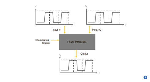
Another benefit of phase interpolator based CDRs is that the data sampling point can be precisely adjusted by a digitally controlled offset. This allows the cancellation of offsets from device mismatches and other causes, and enables in-system measurements of the timing margin available for reliably extracting data from the data signal.

Lastly, although the reference loop can occupy the majority of the area and dissipate the majority of the power in a phase interpolator based CDR, its reference phases can be shared among several CDR loops on chips receiving multiple data signals. In this way, the average size and power required for the CDR functionality per data signal can be greatly reduced.

Who Benefits?

The use of phase interpolator based CDRs benefits many different groups. By designing ASICs including Rambus IO cells that utilize phase interpolator based CDRs, ASIC vendors benefit from the smaller area, lower power, and more stable operation of the IO cells. These benefits are magnified when dual, quad, or other multi-lane IO cells are used since these cells use one reference loop to drive multiple CDR loops for implementing multiple CDRs. The area and power savings can be significant compared to using a PLL per lane, as required by other CDR designs. The ability to digitally offset the data sampling clock when using a phase interpolator based CDR allows in-system testing of timing margins in the actual operating environment. Such system-level testing increases the reliability of manufactured systems for system integrators. Finally, the cost, power, performance, and testability benefits from using phase interpolator based CDRs is passed along to products purchased by consumers in the form of lower prices, longer battery life, and improved reliability.

Output Driver Calibration

Transmitting data at high speeds between a DRAM device and a memory controller requires careful design of IO drivers to ensure that the required electrical signaling levels are achieved. Variations in process, voltage, and temperature can alter the electrical characteristics of the output driver circuitry, resulting in deviations from the desired signaling levels. Additionally, variations in other system elements, such as trace impedance, reference voltage (Vref), and termination voltage (Vterm) can also impact signaling levels. To address these issues, Rambus pioneered the use of Output driver calibration in memory systems to improve communication speeds and provide greater reliability over a wide range of operating conditions.

  • Improves data rates and system voltage margin
  • Increases DRAM yield
  • Compensates for variations in trace impedance and termination voltage
  • Improves system reliability over a wide range of operating conditions

What is Output Driver Calibration Technology?

Comparison of data eye with and without Output Driver Calibration

Variations in process, voltage, and temperature can reduce the size of data eyes. Data eyes reveal characteristics of the quality of the signaling environment such as timing and voltage margins. Robust signaling relies on having wide (good timing margin) and tall (good voltage margin) data eyes. Output drivers are designed to drive signals between high and low voltage levels, shown as Voh and Vol in the previous illustration. Variations in process, voltage, temperature, and other factors can cause output drivers to overshoot and/or undershoot the desired signaling voltage levels, resulting in reduced margins that impact signal integrity. Reduced timing margins limit the maximum signaling speed because the window of time over which the data is valid (width of the data eye) is smaller. Reduced voltage margins can require larger IO voltage swings to ensure accurate transmission of data, but such larger swings result in increased IO power and can increase the sensitivity of the system to cross talk. In order to increase signaling rates and reduce IO power, output driver overshoot and undershoot must be managed.

Output driver calibration allows for optimal signaling levels to be established and maintained using adjustable output drive strengths to compensate for variations in process, voltage, and temperature. Calibrating the output drivers during normal operation allows for drive strength adjustments to respond to changes in voltage and temperature which can fluctuate while a system is in use.

Output Driver Calibration uses feedback that is provided to the output driver circuitry to adjust the output impedance of the output driver circuitry, thereby controlling the circuit’s drive strength.in order to achieve optimal signal performance. The driver’s output impedance is compared to a reference resistor RZQ that is placed off the device. The output impedance is then calibrated to be equal to or proportional to the reference precision resistor.

The circuit above depicts how an Output Driver Calibration circuit may be configured. The voltage dropped across the topmost array of resistors is dependent upon the state of the respective transistors in series with those resistors and the value of the RZQ resistance on the line. The states of the transistors in the transistor array are individually controlled by the Drive Strength Register and are set so that the value of Vterm = Vref. The reference voltage, Vref , is representative of the desired output signal level. When the Vterm = Vref condition is achieved, the impedance in the top of the network divider is optimized for the driver. The values used for configuring the transistor array can be stored in the register and may be updated as needed.

Overshoot and undershoot compensation with Output Driver Calibration

The figure above illustrates the effect that Output Driver Calibration has on the magnitude of overshoot and undershoot along the transmission line. The reduction in overshoot and under-shoot results in increased voltage and timing margins.

The reference resistor RZQ and much of the circuitry for Output Driver Calibration can also be utilized for on-die termination ODT calibration.

Who Benefits?

Output driver calibration provides benefits from the device up through the system. By increasing DRAM yield and allowing DRAM output drivers to automatically compensate for process variation, output driver calibration improves margin and device testability, saving design and test time. Output driver calibration also allows board designers to compensate for variations in trace impedance and termination voltage caused by manufacturing and assembly processes. This ability to compensate for manufacturing tolerances of some components enables test specifications to be relaxed and saves component and tester costs.

At the system level, Output driver calibration enables system integrators to use one DRAM in multiple designs that utilize different trace impedances and that operate in different environments. Output driver calibration also increases voltage and timing margins, resulting in higher system reliability over a wider range of operating conditions. In addition, adjustable drive strengths help compensate for variations in temperature which allows system integrators to more effectively manage their system power and thermal budgets, thereby decreasing overall system cost.

Near Ground Signaling

Reduced power consumption has become of key importance in memory system design—from mobile to enterprise-class applications. In addition to clocking power and DRAM core access power, IO signaling power must be addressed in order to reduce the total power consumption of the memory system. Near ground signaling is a single-ended, ground-terminated technology theat enables high data rates at greatly reduced IO signaling power while reducing design complexity by supporting significantly reduced signal swings of 500 millivolts (mV) and below.

  • Supports high-speed operation with reduced IO signaling power
  • Improved signal integrity
  • Reduced design complexity
  • Eliminates the need for thick-oxide transistors on memory controller
  • Reduced voltage is better matched to advanced processes

What is Near Ground Signaling Technology?

Near Ground Signaling versus SSTL-1.5

Near Ground Signaling (NGS) is a single-ended, ground-terminated signaling technology that enables high data rates at significantly reduced Input Output (IO) signaling power and design complexity, while maintaining excellent signal integrity. With a VDDIO of 0.5V, Near Ground Signaling has a reduced signal swing compared to traditional Stub Series Terminated Logic (SSTL) signaling and lowers IO power on both the DRAM and controller.

This lower IO voltage is better matched to the operating voltage of advanced CPU’s and GPU’s and reduces the cost and complexity of integrating the memory controller on the processor chip.

Who Benefits?

Memory designers benefit from the reduced design complexity, lowering their integrated memory controller implementation costs. They are also able to achieve increased data rates at significantly reduces IO signaling power.

Commercial server managers and consumer end users benefit from the reduced cost of ownership and increased battery life for their end systems and devices.

Module Threading

The growing trend of multi-core processing and converged graphics-compute processors is increasing the performance requirements on the DRAM memory subsystems. Multi-thread computing and graphics not only need higher memory bandwidth but also generate more random accesses to smaller pieces of data. Module Threading improves the throughput and power efficiency of a memory module by applying parallelism to module data accesses. This innovation partitions the module into two individual memory channels and interleaves the commands to each respective channel. The result is a smaller minimum transfer size and reduced row activation power, translating to 50% higher bandwidth and 20% lower memory power compared to a conventional DIMM module.

  • Improves memory throughput up to 50%
  • Reduces power consumption by 20% for equivalent workloads versus conventional modules
  • Enables full utilization of memory IO bandwidth
  • Utilizes conventional DRAM

What is Module Threading Technology?

Threaded module with 2 independently addressable channels

Multi-thread computing is driving up memory bandwidth, but needs smaller access granularity due to the random nature of the data accesses. However, small transfers of data are becoming increasingly difficult with each DRAM generation. Although the memory interface has become faster, the frequency of the main memory core has remained relatively the same. As a result, DRAMs implement core prefetch where a larger amount of data is sensed from the memory core and then serialized to a faster off-chip interface, effectively increasing the access granularity. This discrepancy between the interface speed and the core speed translates to a core-prefetch ratio of 8:1 in current DDR3 DRAMs, and is forecasted to reach 16:1 in future DRAM. This larger prefetch ratio and transfer size can lead to computing inefficiency, especially on multi-threaded and graphics workloads with the need for increased access rate to smaller pieces of data.

The memory subsystem in today’s computing platforms are typically implemented with DIMMs that have a 64bit-wide data bus and a 28bit command/address/clock bus. On a standard DDR3 DIMM module, all the devices within a module rank are accessed simultaneously with a single Command/Address (C/A). An example module configuration places eight (x8) DDR3 components assembled in parallel onto a module printed circuit board and has a minimum efficient data transfer of 64Bytes.

Greater efficiency with a multi-threaded workload and smaller transfers can be achieved by partitioning the module into two separate memory channels, and multiplexing the commands across the same set of traces as a traditional module but with separate chip selects for each respective memory channel. In threaded module, each side of the module is accessed independently, thereby reducing the minimum transfer size to one-half the amount of a standard single-channel module.

Threaded modules can lower the power of main memory accesses. For a conventional eight-device module, all eight DRAMs are activated (ACT) followed by a read or write (COL) operation on all eight devices. A threaded or dual-channel module can accomplish the same data transfer by activating only four devices and then performing two consecutive read or write operations to those devices. Since only four devices are activated per access instead of eight devices, a threaded or dual-channel module achieves equivalent bandwidth with one-half the device row activation power. On a memory system, this translates to approximately 20% reduced total module power.

Sustained bandwidth comparison of conventional and threaded modules

Another benefit that threaded modules offer is increased sustained bandwidth at high data rates. Many modern industry-standard DRAMs have limited bandwidth due to power restrictions on the DRAM devices. On DRAMs starting with the DDR3 generation, only a limited number of banks may be accessed in order to protect the on–DRAM power delivery network and maintain a stable voltage for the memory core. This parameter, know as tFAW (Four Activate Window period) allows only 4 banks to be activated in the rolling tFAW window.

For a computing system, tFAW restricts the memory controller from issuing additional row activate commands once four activates have already been issued in a given tFAW period. This stalls the memory controller and results in lost data bandwidth. A DDR3 DRAM running at 1600Mbps data rates loses up to 50% of its sustained data bandwidth due to this and other restrictions. Since the DRAMs in a threaded module are activated half as often as those in a conventional module, the sustained bandwidth of a threaded module is not limited by the core parameters.

Who Benefits?

Module threading delivers system designers the benefits of increased bandwidth from improved transfer efficiency and smaller access granularity, while maintaining the commodity cost structure of the module. End users can benefit from the 50% improvement in throughput performance as well as the 20% reduction in total memory power.

FlexPhase™ Timing Adjustment Circuits

Precise on-chip alignment of data clock are crucial for today’s high performance memory systems. In addition, offsets in timing caused by variations in process, voltage and timing must be accounted for. FlexPhase™ Timing Adjustment Circuits are a key technology ingredient for achieving high data rates on chip-to-chip systems that reference an external clock signal. By calibrating the signal phase offsets at the bit or byte level, FlexPhase timing adjustments eliminate many timing differences associated with process variations, driver/receiver mismatch, on-chip clock skew and clock standing wave effects, as well as the need for trace length matching.

  • Simplifies high-speed system design
  • Eliminates requirements for trace length matching and reduce routing area requirements
  • Optimizes IO signal timing for improved timing margins
  • Complements Fly-by command/address system architectures

What is FlexPhase Technology?

FlexPhase™ per-pin timing adjustment

FlexPhase technology anticipates the phase difference between signals on different traces and manages the transmission of data bits so that the data arrives at the memory device with a known timing relationship with respect to the command and address signals sent to the memory device. It can also be used to enhance conventional DRAM architectures by managing the variation in signal propagation times due to variations in trace lengths.

In DRAM systems, FlexPhase circuits can be used to optimize data and strobe placement. FlexPhase circuits can also be used to finely tune the timing relationships between data, command, address and clock signals. In conventional DRAM architectures, FlexPhase circuits can be used to deskew incoming signals at the controller in order to compensate for uncertainty in the arrival times of signals. Further, FlexPhase circuits can be used to intentionally inject a timing offset – “preskew” data such that the data will arrive at the DRAM devices coincident with the command/address or clock signal. FlexPhase minimizes the systematic timing errors in typical memory systems by adjusting transmit and receive phase offsets at each pin or pin-group.

When using a Fly-by architecture, the amount of time required for the data, strobe, command, address and clock signals to propagate between the memory controller and DRAMs is primarily affected by the lengths of the traces between the controller and the DRAM devices over which the signals propagate. In a Fly-by system, the command, address and clock signals arrive at each DRAM at different times, which in turn results in the data signals being transmitted from each DRAM device at different times. FlexPhase can be used at the controller to deskew those data signals to eliminate the offset due to the Fly-by architecture in addition to any inherent timing offsets of the system. Similarly, because the command, address and clock signals arrive at each DRAM at different times, the data for write operations to the memory devices needs to be preskewed by the controller to account for the difference in when the memory devices will be expecting the write data. FlexPhase can accomplish that preskewing while still eliminating inherent timing offsets in the system.

FlexPhase is a departure from traditional serial link technologies in which timing deskew is performed using an embedded clock. Such deskewing techniques, which typically rely on 8b/10b encoding to ensure adequate transition density for clock recovery, require more chip area, have added power consumption, increase latency, and suffer a 20 percent bandwidth penalty associated with the 8b/10b encoding.

FlexPhase includes in-system timing characterization and self-test functionality that enables aggressive timing.

Example of system employing

During READ access operations, a memory controller incorporating FlexPhase technology determines and stores the “receive” phase difference between the transmitted control signals and the data received from each memory device. The phase difference corresponding to each memory device is subsequently used to deskew the data signals which arrive at the memory controller at different times, thereby allowing proper reconstitution of the data accessed from each of the memory devices.

During WRITE operations, a similar process is performed where a “transmit” phase difference is determined for each memory device and stored within the memory controller. Those transmit phase differences are then used to modify (preskew) the timing delay between the transmitted command/address signals and the data sent to each memory device.

Who Benefits?

FlexPhase circuit technology brings flexibility, simplicity, and savings to memory system designers. At the device level, FlexPhase technology helps to compensate for the manufacturing variations that degrade timing windows and operational performance of the memory. The FlexPhase approach allows memory interfaces to operate at GHz rates without the power, area and latency penalties incurred in systems using Clock and Data Recovery (CDR) techniques. FlexPhase also provides for improved testability by using digital phase offsets for margin testing of the high speed chip interfaces—saving design time and cost.

At the system level, FlexPhase technology relaxes PCB trace length matching requirements by anticipating and calibrating the signaling phase offsets caused by variations in trace lengths and impedances. FlexPhase timing adjustments allows much simpler, more compact and cost-efficient memory layouts. FlexPhase timing adjustments provide for in-system test and characterization of key data signals, thereby enabling performance testing of the high speed links.

Double Bus Rate Technology

In many computing systems today, memory bandwidth is a key factor in determining overall system performance, and its importance continues to grow as these systems evolve. Rambus developed a technique for improving memory system bandwidth by increasing the per-pin signaling rate of the data pins of the DRAM. Double Data Rate (DDR) SDRAMs are an example of memory devices that double the per-pin data signaling rate by transferring data on both edges during each clock cycle instead of only on one edge. While such an increase in signaling rate can improve memory bandwidth of the data pins, actual system performance may not improve due to insufficient address/control bandwidth that can reduce data transfer efficiency. To address this problem, Rambus developed Double Bus Rate Technology, an innovation that increases both address/control, and data bandwidth, allowing memory systems to achieve higher levels of performance.

  • Increases transfer rate without increase system clock rates
  • Improves memory system bandwidth

What is Double Bus Rate Technology?

Single data rate and double data rate read transactions

In a read transaction for a single data rate DRAM, the address, control, and data is transferred on one edge of each clock cycle. Memory bandwidth can be improved by applying double bus rate technology and increasing the per-pin data signaling rate of a DRAM. Double Bus Rate Technology allows data to be transferred more quickly, increasing the bandwidth that a DRAM can supply.

Interleaved double date rate read transactions without Double Bus Rate technology

Doubling the data rate of the data transfers affects the relationship between address/control information and data for a Read transaction. When transactions are interleaved, a problem can occur when the amount of time that data occupies the memory bus is smaller than the amount of time that address and control information occupy the bus. In this situation, the insufficient address/control bandwidth leads to bubbles in the data transfer on the bus, resulting in reduced memory bandwidth and loss of performance.

Interleaved double bus rate read transactions without Double Bus Rate technology

The issue of performance loss can be addressed by applying Double Bus Rate Technology to the address and control pins as well. Double Bus Rate Technology is used to balance address, control, and data bandwidth, thereby eliminating the concerns relating to insufficient address and control bandwidth. As a result, bandwidth is increased by 50% compared to the interleaved transactions with double bus rate technology. Another example of where increased control bandwidth can be useful is in systems that use write masking. In systems that utilize write masking, increasing the amount of data being transferred to memory requires that more byte masking control information be specified in order to maintain support for data masking at byte granularities. By balancing address, control, and data transfer rates on the bus with Double Bus Rate Technology, performance losses due to insufficient address and control bandwidth are eliminated.

Who Benefits?

Many groups can benefit from double bus rate technology. By balancing address, control, and data bandwidth, system designers are able to achieve the highest levels of memory bandwidth in their systems. This in turn helps to reduce the number of DRAMs necessary to achieve a given level of memory performance, reducing component count and easing system component placement, routing concerns, and thermal dissipation. System designers and integrators benefit from the reduced component count needed to achieve a given level of memory bandwidth, resulting in lower system cost and smaller form-factor systems.

  • Go to page 1
  • Go to page 2
  • Go to page 3
  • Go to page 4
  • Go to Next Page »

Footer

About

  • Corporate Overview
  • Leadership
  • Careers
  • Locations
  • Investor Relations
  • News
  • Corporate Responsibility

Products

  • Memory PHYs
  • SerDes PHYs
  • Digital Controllers
  • Server DIMM Chipsets
  • Root of Trust Solutions
  • Provisioning and Key Management
  • Protocol Engines
  • Crypto Accelerator Cores
  • Software Protocols
  • DPA Countermeasures
  • Anti-Counterfeiting
  • CryptoMedia

Markets

  • AI & Machine Learning
  • Automotive
  • Data Center
  • Edge
  • Government
  • IoT
  • Pay TV

Resources

  • Resource Library
  • Webinars
  • Inventions
  • Buying Guide
  • Contact

Copyright © 2023 Rambus.com. All Rights Reserved. Privacy Policy | Trademark & Guidelines

  • Facebook icon
  • Twitter icon
  • YouTuve icon
  • LinkedIn icon
  • Blog icon