• Skip to primary navigation
  • Skip to main content
  • Skip to footer
  • enEnglish
  • Investor Relations
  • Resource Library
  • Newsroom
  • Blog
  • Careers
  • Support Center
Rambus Logo

Rambus

At Rambus, we create cutting-edge semiconductor and IP products, spanning memory and interfaces to security, smart sensors and lighting.

  • Products
      • All
          • Interface IP
          • Memory PHYs
          • GDDR6 PHY
          • HBM2E PHY
          • DDR4 PHY
          • More…
          • SerDes PHYs
          • PCIe 5.0 PHY
          • PCIe 4.0 PHY
          • 112G LR PHY
          • 112G XSR PHY
          • 56G PHY
          • 32G PHY
          • 28G PHY
          • More…
          • Northwest Logic Controllers
          • Memory Controllers
          • PCI Express Controllers
          • MIPI Controllers
          • Security IP
          • Root of Trust Solutions
          • Provisioning and Key Management
          • CryptoManager Provisioning
          • CryptoManager Device Key Management
          • Protocol Engines
          • MACsec Engines
          • Multi-Protocol Engines
          • Crypto Accelerator Cores
          • DPA Resistant Cores
          • Basic Crypto Blocks
          • DPA Countermeasures
          • Software Protocols & Crypto Toolkits
          • Anti-Counterfeiting
          • Memory Interface Chips
          • Server DIMM Chipsets
          • DDR5 DIMM Chipset
          • DDR4 NVRCD
          • DDR4 Register Clock Driver
          • DDR4 Data Buffer
          • More…
      • Interface IP
          • Memory PHYs
            • GDDR6 PHY
            • HBM2E PHY
            • DDR4 PHY
            • DDR4 Multi-modal PHY
            • DDR3 PHY
          • SerDes PHYs
            • PCIe 5.0 PHY
            • PCIe 4.0 PHY
            • 112G LR PHY
            • 112G XSR PHY
            • 56G PHY
            • 32G PHY
            • 28G PHY
            • 16G PHY
            • 12G PHY
            • 6G PHY
          • Northwest Logic Controllers
            • PCIe 5.0 Controller
            • PCIe 4.0 Controller
            • HBM2E Controller
            • GDDR6 Controller
            • LPDDR4 Controller
            • DDR4 Controller
            • DDR3 Controller
            • MIPI DSI-2 Controller Core
            • MIPI CSI-2 Controller Core

        • With their reduced power consumption and industry-leading data rates, our line-up of memory interface IP solutions support a broad range of industry standards with improved margin and flexibility. Learn more about our Interface IP solutions
      • Security IP
          • Root of Trust
          • Provisioning and Key Management
            • CryptoManager Provisioning
            • CryptoManager Device Key Management
            • Secure Silicon Provisioning
            • Secure Device Provisioning
          • Protocol Engines
            • MACsec Engines
            • Multi-Protocol Engines for IPsec, TLS and SSL
            • High Speed Public Key Accelerator
          • Crypto Accelerator Cores
            • DPA Resistant Cores
            • Basic Crypto Blocks
          • Anti-Counterfeiting
            • CryptoFirewall Cores
            • Circuit Camouflage Technology
          • DPA Countermeasures
            • DPA Resistant Cores
            • DPA Resistant Software Libraries
            • DPA Workstation Platform
          • Software Protocols & Crypto Toolkits
            • Cloud-optimized IPsec Toolkit
            • Secure Communication Toolkits
            • IoT Security Framework
          • CryptoMedia
            • Content Protection Core
            • Content Protection Services

        • From chip-to-cloud-to-crowd, Rambus secure silicon IP helps protect the world’s most valuable resource: data. Securing electronic systems at their hardware foundation, our embedded security solutions span areas including root of trust, tamper resistance, content protection and trusted provisioning. Learn more about our Security IP offerings
      • Memory Interface Chips
        • Server DIMM Chipsets
          • DDR5 DIMM Chipset
          • Non-Volatile DDR4 Registering Clock Driver
          • DDR4 Register Clock Driver
          • DDR4 Data Buffer
          • DDR3 Register Clock Driver
          • DDR3 Isolation Memory Buffer

        • Made for high speed, reliability and power efficiency, our DDR3, DDR4, and DDR5 chipsets for RDIMM and LRDIMM server modules deliver top-of-the-line performance and capacity for the next wave of enterprise and data center servers. Learn more about our Memory Interface Chip solutions
  • Markets
      • AI & Machine Learning
        • Speed and Security for the Artificial Intelligence & Machine Learning Revolution
          • Products
          • SerDes PHYs
          • Memory PHYs
          • Digital Controllers
          • Memory Interface Chips
          • Root of Trust
          • Crypto Accelerator Cores
          • Protocol Engines
          • Provisioning and Key Management
          • AI & Machine Learning
      • Automotive
        • Providing Performance & Security for the Connected Car
          • Products
          • Memory PHYs
          • SerDes PHYs
          • Digital Controllers
          • Root of Trust
          • PKE Engine
          • MACsec Engines
          • Crypto Accelerator Cores
          • Provisioning and Key Management
          • Explore Automotive
      • Data Center
        • Optimizing capacity, connectivity and capability of the cloud
          • Products
          • SerDes PHYs
          • Memory PHYs
          • Digital Controllers
          • Memory Interface Chips
          • Root of Trust
          • MACsec Engines
          • Software Protocols
          • Provisioning and Key Management
          • See Data Center
      • Edge
        • Catching a tidal wave of data
          • Products
          • Memory PHYs
          • SerDes PHYs
          • Digital Controllers
          • Root of Trust
          • Crypto Accelerator Cores
          • Protocol Engines
          • Software Protocols
          • Discover Edge
      • Government
        • Securing Mission-critical Systems
          • Products
          • Root of Trust
          • Protocol Engines
          • Anti-Tamper Cores
          • Provisioning and Key Management
          • DPA Workstation Platform
          • SerDes PHYs
          • Memory PHYs
          • Digital Controllers
          • See Government
      • IoT
        • Making IoT Data Safe & Fast
          • Products
          • Root of Trust
          • TLS Toolkits
          • Provisioning and Key Management
          • Memory PHYs
          • SerDes PHYs
          • Digital Controllers
          • Explore IoT
  • Resources
    • Inventions
    • Buying Guide
    • Resource Library
      • Webinars
  • About
      • Corporate Overview
      • Leadership
      • Inventors
      • Careers
      • Locations
      • Investor Relations
      • Newsroom
      • Blog
      • Events
      • Partnerships
      • Corporate Social Responsibility
      • Contact
Home > Inventions > Memory + Interfaces > Output Driver Calibration

Output Driver Calibration

Transmitting data at high speeds between a DRAM device and a memory controller requires careful design of IO drivers to ensure that the required electrical signaling levels are achieved. Variations in process, voltage, and temperature can alter the electrical characteristics of the output driver circuitry, resulting in deviations from the desired signaling levels. Additionally, variations in other system elements, such as trace impedance, reference voltage (Vref), and termination voltage (Vterm) can also impact signaling levels. To address these issues, Rambus pioneered the use of Output driver calibration in memory systems to improve communication speeds and provide greater reliability over a wide range of operating conditions.

  • Improves data rates and system voltage margin
  • Increases DRAM yield
  • Compensates for variations in trace impedance and termination voltage
  • Improves system reliability over a wide range of operating conditions

What is Output Driver Calibration Technology?

Comparison of data eye with and without Output Driver Calibration

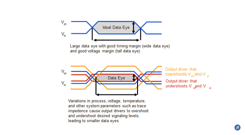
Variations in process, voltage, and temperature can reduce the size of data eyes. Data eyes reveal characteristics of the quality of the signaling environment such as timing and voltage margins. Robust signaling relies on having wide (good timing margin) and tall (good voltage margin) data eyes. Output drivers are designed to drive signals between high and low voltage levels, shown as Voh and Vol in the previous illustration. Variations in process, voltage, temperature, and other factors can cause output drivers to overshoot and/or undershoot the desired signaling voltage levels, resulting in reduced margins that impact signal integrity. Reduced timing margins limit the maximum signaling speed because the window of time over which the data is valid (width of the data eye) is smaller. Reduced voltage margins can require larger IO voltage swings to ensure accurate transmission of data, but such larger swings result in increased IO power and can increase the sensitivity of the system to cross talk. In order to increase signaling rates and reduce IO power, output driver overshoot and undershoot must be managed.

Output driver calibration allows for optimal signaling levels to be established and maintained using adjustable output drive strengths to compensate for variations in process, voltage, and temperature. Calibrating the output drivers during normal operation allows for drive strength adjustments to respond to changes in voltage and temperature which can fluctuate while a system is in use.

Output Driver Calibration uses feedback that is provided to the output driver circuitry to adjust the output impedance of the output driver circuitry, thereby controlling the circuit’s drive strength.in order to achieve optimal signal performance. The driver’s output impedance is compared to a reference resistor RZQ that is placed off the device. The output impedance is then calibrated to be equal to or proportional to the reference precision resistor.

The circuit above depicts how an Output Driver Calibration circuit may be configured. The voltage dropped across the topmost array of resistors is dependent upon the state of the respective transistors in series with those resistors and the value of the RZQ resistance on the line. The states of the transistors in the transistor array are individually controlled by the Drive Strength Register and are set so that the value of Vterm = Vref. The reference voltage, Vref , is representative of the desired output signal level. When the Vterm = Vref condition is achieved, the impedance in the top of the network divider is optimized for the driver. The values used for configuring the transistor array can be stored in the register and may be updated as needed.

Overshoot and undershoot compensation with Output Driver Calibration

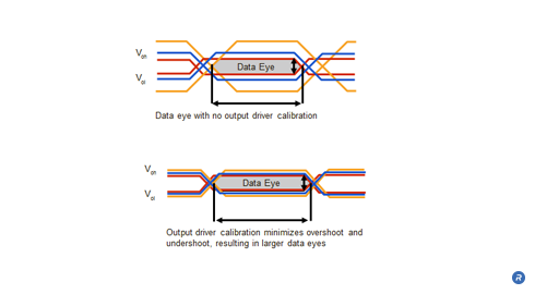
The figure above illustrates the effect that Output Driver Calibration has on the magnitude of overshoot and undershoot along the transmission line. The reduction in overshoot and under-shoot results in increased voltage and timing margins.

The reference resistor RZQ and much of the circuitry for Output Driver Calibration can also be utilized for on-die termination ODT calibration.

Who Benefits?

Output driver calibration provides benefits from the device up through the system. By increasing DRAM yield and allowing DRAM output drivers to automatically compensate for process variation, output driver calibration improves margin and device testability, saving design and test time. Output driver calibration also allows board designers to compensate for variations in trace impedance and termination voltage caused by manufacturing and assembly processes. This ability to compensate for manufacturing tolerances of some components enables test specifications to be relaxed and saves component and tester costs.

At the system level, Output driver calibration enables system integrators to use one DRAM in multiple designs that utilize different trace impedances and that operate in different environments. Output driver calibration also increases voltage and timing margins, resulting in higher system reliability over a wider range of operating conditions. In addition, adjustable drive strengths help compensate for variations in temperature which allows system integrators to more effectively manage their system power and thermal budgets, thereby decreasing overall system cost.

Footer

About

  • Corporate Overview
  • Leadership
  • Careers
  • Locations
  • Investor Relations
  • News
  • Corporate Social Responsibility

Products

  • Memory PHYs
  • SerDes PHYs
  • Northwest Logic Controllers
  • Server DIMM Chipsets
  • Root of Trust Solutions
  • Provisioning and Key Management
  • Protocol Engines
  • Crypto Accelerator Cores
  • Software Protocols
  • DPA Countermeasures
  • Anti-Counterfeiting
  • CryptoMedia

Markets

  • AI & Machine Learning
  • Automotive
  • Data Center
  • Edge
  • Government
  • IoT
  • Pay TV

Resources

  • Resource Library
  • Webinars
  • Inventions
  • Buying Guide
  • Contact

Copyright © 2021 Rambus.com. All Rights Reserved. Privacy Policy | Trademark & Guidelines

  • Facebook icon
  • Twitter icon
  • YouTuve icon
  • LinkedIn icon
  • Blog icon