• Skip to primary navigation
  • Skip to main content
  • Skip to footer
  • English
  • Investor Relations
  • Resource Library
  • Newsroom
  • Blog
  • Careers
  • Support Center
Rambus Logo

Rambus

At Rambus, we create cutting-edge semiconductor and IP products, spanning memory and interfaces to security, smart sensors and lighting.

  • Products
      • All
          • Memory Interface Chips
          • DIMM Chipsets
          • DDR5 DIMM Chipset
          • DDR4 NVRCD
          • DDR4 Register Clock Driver
          • DDR4 Data Buffer
          • CXL Memory Interconnect Initiative
          • Interface IP
          • Memory PHYs
          • GDDR6 PHY
          • HBM3 PHY
          • HBM2E PHY
          • DDR4 PHY
          • More…
          • SerDes PHYs
          • PCIe 6.0 PHY
          • PCIe 5.0 PHY
          • 32G C2C PHY
          • 32G PHY
          • 28G PHY
          • More…
          • Digital Controllers
          • Memory Controllers
          • CXL & PCI Express Controllers
          • MIPI Controllers
          • Video Compression and Forward Error Correction Cores
          • Security IP
          • Root of Trust Solutions
          • Security Protocol Engines
          • Inline Cipher Engines
          • Crypto Accelerator Cores
          • DPA Countermeasures
          • Software Protocols & Crypto Toolkits
          • Anti-Counterfeiting
          • Provisioning and Key Management
      • Memory Interface Chips
        • DIMM Chipsets
          • DDR5 DIMM Chipset
          • Non-Volatile DDR4 Registering Clock Driver
          • DDR4 Register Clock Driver
          • DDR4 Data Buffer
          • DDR3 Register Clock Driver
          • DDR3 Isolation Memory Buffer
        • CXL Memory Interconnect Initiative

        • Made for high speed, reliability and power efficiency, our DDR3, DDR4, and DDR5 DIMM chipsets deliver top-of-the-line performance and capacity for the next wave of computing systems. Learn more about our Memory Interface Chip solutions
      • Interface IP
          • Memory PHYs
            • GDDR6 PHY
            • HBM3 PHY
            • HBM2E PHY
            • DDR4 PHY
            • DDR4 Multi-modal PHY
            • DDR3 PHY
          • SerDes PHYs
            • PCIe 6.0 PHY
            • PCIe 5.0 PHY
            • PCIe 4.0 PHY
            • 32G C2C PHY
            • 32G PHY
            • 28G PHY
            • 16G PHY
            • 12G PHY
            • 6G PHY
          • Digital Controllers
            • HBM3 Controller
            • HBM2E Controller
            • GDDR6 Controller
            • LPDDR5 Controller
            • CXL 2.0 Controller
            • PCIe 6.0 Controller
            • PCIe 5.0 Controller
            • MIPI CSI-2/DSI-2 Controllers
            • Video Compression and Forward Error Correction Cores
            • More…

        • With their reduced power consumption and industry-leading data rates, our line-up of memory interface IP solutions support a broad range of industry standards with improved margin and flexibility. Learn more about our Interface IP solutions
      • Security IP
          • Root of Trust Solutions
          • Security Protocol Engines
            • MACsec Engines
            • IPsec, TLS, SSL Multi-Protocol Engines
            • High Speed Public Key Accelerator
          • Inline Cipher Engines
          • Crypto Accelerator Cores
            • DPA Resistant Cores
            • Basic Crypto Blocks
          • Anti-Counterfeiting
            • CryptoFirewall Cores
            • Circuit Camouflage Technology
          • DPA Countermeasures
            • DPA Resistant Cores
            • DPA Resistant Software Libraries
            • DPA Workstation Platform
          • Software Protocols & Crypto Toolkits
            • IPsec Toolkit
            • FIPs Cryptographic Libraries
            • MACsec Toolkit
            • IoT Security Framework
          • CryptoMedia
            • Content Protection Core
            • Content Protection Services
          • Provisioning and Key Management
            • CryptoManager Provisioning
            • CryptoManager Device Key Management

        • From chip-to-cloud-to-crowd, Rambus secure silicon IP helps protect the world’s most valuable resource: data. Securing electronic systems at their hardware foundation, our embedded security solutions span areas including root of trust, tamper resistance, content protection and trusted provisioning. Learn more about our Security IP offerings
  • Markets
      • AI & Machine Learning
        • Speed and Security for the Artificial Intelligence & Machine Learning Revolution
          • Products
          • SerDes PHYs
          • Memory PHYs
          • Digital Controllers
          • Memory Interface Chips
          • Root of Trust
          • Crypto Accelerator Cores
          • Protocol Engines
          • Provisioning and Key Management
          • AI & Machine Learning
      • Automotive
        • Providing Performance & Security for the Connected Car
          • Products
          • Memory PHYs
          • SerDes PHYs
          • Digital Controllers
          • Root of Trust
          • PKE Engine
          • MACsec Engines
          • Crypto Accelerator Cores
          • Provisioning and Key Management
          • Explore Automotive
      • Data Center
        • Optimizing capacity, connectivity and capability of the cloud
          • Products
          • SerDes PHYs
          • Memory PHYs
          • Digital Controllers
          • Memory Interface Chips
          • Root of Trust
          • MACsec Engines
          • Software Protocols
          • Provisioning and Key Management
          • See Data Center
      • Edge
        • Catching a tidal wave of data
          • Products
          • Memory PHYs
          • SerDes PHYs
          • Digital Controllers
          • Root of Trust
          • Crypto Accelerator Cores
          • Protocol Engines
          • Software Protocols
          • Discover Edge
      • Government
        • Securing Mission-critical Systems
          • Products
          • Root of Trust
          • Protocol Engines
          • Anti-Tamper Cores
          • Provisioning and Key Management
          • DPA Workstation Platform
          • SerDes PHYs
          • Memory PHYs
          • Digital Controllers
          • See Government
      • IoT
        • Making IoT Data Safe & Fast
          • Products
          • Root of Trust
          • TLS Toolkits
          • Provisioning and Key Management
          • Memory PHYs
          • SerDes PHYs
          • Digital Controllers
          • Explore IoT
  • Resources
    • Inventions
    • Buying Guide
    • Resource Library
      • Webinars
      • Product Selector
  • About
      • Corporate Overview
      • Leadership
      • Inventors
      • Careers
      • Locations
      • Investor Relations
      • Newsroom
      • Blog
      • Events
      • Partnerships
      • Certifications
      • Corporate Responsibility
      • Contact
Home > Inventions > Memory + Interfaces > FlexPhase™ Timing Adjustment Circuits

FlexPhase™ Timing Adjustment Circuits

Precise on-chip alignment of data clock are crucial for today’s high performance memory systems. In addition, offsets in timing caused by variations in process, voltage and timing must be accounted for. FlexPhase™ Timing Adjustment Circuits are a key technology ingredient for achieving high data rates on chip-to-chip systems that reference an external clock signal. By calibrating the signal phase offsets at the bit or byte level, FlexPhase timing adjustments eliminate many timing differences associated with process variations, driver/receiver mismatch, on-chip clock skew and clock standing wave effects, as well as the need for trace length matching.

  • Simplifies high-speed system design
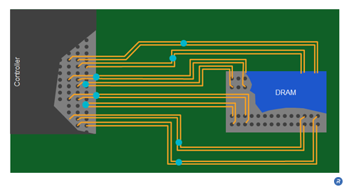
  • Eliminates requirements for trace length matching and reduce routing area requirements
  • Optimizes IO signal timing for improved timing margins
  • Complements Fly-by command/address system architectures

What is FlexPhase Technology?

FlexPhase™ per-pin timing adjustment

FlexPhase technology anticipates the phase difference between signals on different traces and manages the transmission of data bits so that the data arrives at the memory device with a known timing relationship with respect to the command and address signals sent to the memory device. It can also be used to enhance conventional DRAM architectures by managing the variation in signal propagation times due to variations in trace lengths.

In DRAM systems, FlexPhase circuits can be used to optimize data and strobe placement. FlexPhase circuits can also be used to finely tune the timing relationships between data, command, address and clock signals. In conventional DRAM architectures, FlexPhase circuits can be used to deskew incoming signals at the controller in order to compensate for uncertainty in the arrival times of signals. Further, FlexPhase circuits can be used to intentionally inject a timing offset – “preskew” data such that the data will arrive at the DRAM devices coincident with the command/address or clock signal. FlexPhase minimizes the systematic timing errors in typical memory systems by adjusting transmit and receive phase offsets at each pin or pin-group.

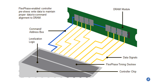
When using a Fly-by architecture, the amount of time required for the data, strobe, command, address and clock signals to propagate between the memory controller and DRAMs is primarily affected by the lengths of the traces between the controller and the DRAM devices over which the signals propagate. In a Fly-by system, the command, address and clock signals arrive at each DRAM at different times, which in turn results in the data signals being transmitted from each DRAM device at different times. FlexPhase can be used at the controller to deskew those data signals to eliminate the offset due to the Fly-by architecture in addition to any inherent timing offsets of the system. Similarly, because the command, address and clock signals arrive at each DRAM at different times, the data for write operations to the memory devices needs to be preskewed by the controller to account for the difference in when the memory devices will be expecting the write data. FlexPhase can accomplish that preskewing while still eliminating inherent timing offsets in the system.

FlexPhase is a departure from traditional serial link technologies in which timing deskew is performed using an embedded clock. Such deskewing techniques, which typically rely on 8b/10b encoding to ensure adequate transition density for clock recovery, require more chip area, have added power consumption, increase latency, and suffer a 20 percent bandwidth penalty associated with the 8b/10b encoding.

FlexPhase includes in-system timing characterization and self-test functionality that enables aggressive timing.

Example of system employing

During READ access operations, a memory controller incorporating FlexPhase technology determines and stores the “receive” phase difference between the transmitted control signals and the data received from each memory device. The phase difference corresponding to each memory device is subsequently used to deskew the data signals which arrive at the memory controller at different times, thereby allowing proper reconstitution of the data accessed from each of the memory devices.

During WRITE operations, a similar process is performed where a “transmit” phase difference is determined for each memory device and stored within the memory controller. Those transmit phase differences are then used to modify (preskew) the timing delay between the transmitted command/address signals and the data sent to each memory device.

Who Benefits?

FlexPhase circuit technology brings flexibility, simplicity, and savings to memory system designers. At the device level, FlexPhase technology helps to compensate for the manufacturing variations that degrade timing windows and operational performance of the memory. The FlexPhase approach allows memory interfaces to operate at GHz rates without the power, area and latency penalties incurred in systems using Clock and Data Recovery (CDR) techniques. FlexPhase also provides for improved testability by using digital phase offsets for margin testing of the high speed chip interfaces—saving design time and cost.

At the system level, FlexPhase technology relaxes PCB trace length matching requirements by anticipating and calibrating the signaling phase offsets caused by variations in trace lengths and impedances. FlexPhase timing adjustments allows much simpler, more compact and cost-efficient memory layouts. FlexPhase timing adjustments provide for in-system test and characterization of key data signals, thereby enabling performance testing of the high speed links.

Footer

About

  • Corporate Overview
  • Leadership
  • Careers
  • Locations
  • Investor Relations
  • News
  • Corporate Responsibility

Products

  • Memory PHYs
  • SerDes PHYs
  • Digital Controllers
  • Server DIMM Chipsets
  • Root of Trust Solutions
  • Provisioning and Key Management
  • Protocol Engines
  • Crypto Accelerator Cores
  • Software Protocols
  • DPA Countermeasures
  • Anti-Counterfeiting
  • CryptoMedia

Markets

  • AI & Machine Learning
  • Automotive
  • Data Center
  • Edge
  • Government
  • IoT
  • Pay TV

Resources

  • Resource Library
  • Webinars
  • Inventions
  • Buying Guide
  • Contact

Copyright © 2023 Rambus.com. All Rights Reserved. Privacy Policy | Trademark & Guidelines

  • Facebook icon
  • Twitter icon
  • YouTuve icon
  • LinkedIn icon
  • Blog icon