As the performance requirements of digital systems continue to increase, there are increasing requirements to deliver signal integrity that enables reliable operation at higher signaling rates. Signal line terminations are useful elements in the management of signal integrity, and can be use external to the memory device or within the device itself. Incorporating a resistive termination within the DRAM device, which is often referred to as On Die Termination (ODT), improves the signaling environment by reducing the electrical discontinuities introduced with off-die termination. However, variations across process, voltage and temperature (PVT) can cause instability in the resistive characteristics of the ODT elements. Rambus ODT Calibration determines an optimal termination impedance to reduce signal reflections and compensate for variations across PVT.
- Calibrates ODT termination impedance
- Reduces signal reflections
- Compensates for variations across PVT and operating conditions
What is On Die Termination Calibration Technology?
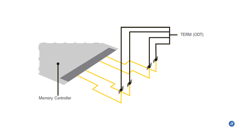
Conventional DRAM memory module architectures typically include line termination resistors on the motherboard. Although the termination resistors on the motherboard reduce some reflections on the signal lines, they are unable to prevent reflections resulting from the stub lines that connect to the DRAMs on the module. A signal propagating from the memory controller to the DRAM encounters an impedance discontinuity at the stub leading to the DRAM on the module. The signal that propagates along the stub to the DRAM will be reflected back onto the signal line, thereby introducing unwanted noise into the signal. The introduced noise and the consequential signal degradations that are not addressed by such off-die termination become more pronounced with higher data rates and longer stub lengths. Larger, multi-drop systems containing multiple DRAM modules introduce even more reflections and consequently add more reflective noise, thereby resulting in further signal degradation.
By placing the termination resistance on the die itself rather than the motherboard, the reflections resulting from discontinuities in the line are significantly reduced, thus producing a cleaner signal and enabling faster data rates.
ODT calibration is a technique that involves calibrating the termination impedance in order to optimize the reduction of signal reflections. ODT calibration allows an optimal termination value to be established that compensates for variations in process and operating conditions.
A calibrated ODT value significantly reduces unwanted signal reflections while only minimally attenuating the magnitude of the signal swing due to the added resistive loading. The resulting cleaner data signal allows for higher data rates.
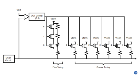
ODT calibration is achieved by establishing an ODT impedance that is proportional to an external precision resistor. The same external resistor can also be used for Output Driver Calibration.
The ODT calibration controller, compares the voltage drop across the ODT resistor network with a voltage drop across an external resistor represented. The controller modifies the resistor network with coarse tuning and fine tuning to achieve an impedance value that closely approximates the external, reference resistance.
Who Benefits?
ODT calibration delivers benefits at the device, subsystem and system level. By implementing ODT calibration, devices are able to achieve enhanced signal performance and higher data rates, which enables designers to achieve superior DRAM device and module performance.
In addition, placing the termination components on the DRAM devices removes these elements from the PCB. In doing so, the number of components and signal lines on the motherboard is reduced, lowering the cost and complexity while increasing reliability.
Finally, the system benefits from the superior data rates and module performance that are enabled through the improved signal integrity achieved with ODT calibration.