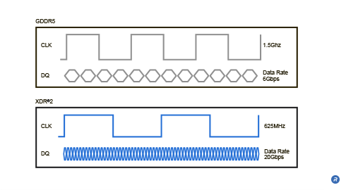
As memory systems continue to evolve, memory system bandwidth is advancing to higher levels through the use of wider memory system buses and faster per-pin signaling rates. Controller package cost, motherboard routing complexity, and system space constraints make further increases in memory bus widths difficult, and result in an increased emphasis on improving per-pin signaling rates in memory systems.
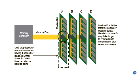
Conventional systems support capacity upgrades with multiple modules using multi-drop topologies—attaching multiple devices per data bus wire. However, each device and longer bus wires add capacitive loading to the memory bus which reduces signal integrity and the maximum signaling rate of the system. The trade-off then becomes capacity or speed.
Buffered modules eliminate this trade-off by enabling memory bus speeds to increase and support multiple modules while reducing capacitive loading by electrically isolating the DRAMs from the memory bus.
- Enables high-bandwidth, high-capacity memory systems
- Supports multiple module capacity upgrades without degrading per pin data rates
- Reduces memory bus width requirements and motherboard routing complexity
- Reduces IO pin count and package cost
What are Buffered Modules?
Buffered modules introduce a memory buffer between the memory controller and the DRAM devices on each module, isolating the DRAM from the memory bus and enabling an increase to the width of the memory without increasing the pin count of the controller. This also reduces the effective capacitive load on the memory bus enabling support for multiple modules at high speed.

Unlike conventional approaches that limit bus lengths and the number of modules supported, buffered modules support high memory capacity through increased numbers of memory modules. Conventional unbuffered memory systems that support DDRn SDRAM can have multiple capacitive loads on the memory bus. Each data bus wire can have up to 2 capacitive loads per memory module (one from a DRAM on the front of the module, and one from a DRAM on the back of the module in the case of a double-sided module). As the number of modules supported on the memory bus increases, the potential capacitive loading on the bus also increases. Buffered modules reduce this capacitive load by routing the memory bus to a single buffer per module rather than each individual device.

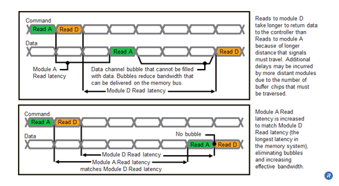
Buffered modules also provide the added benefit of being able to compensate for signal attenuation and latency between the memory controller and modules without introducing additional pins to the controller. The modules that are more physically distant from the memory controller than others will have higher access latencies than those that are closer to the controller at high speeds. Because of this variation in access latency, back-to-back memory references that access different modules may incur a “bubble” on the memory bus, resulting in a loss of efficiency. To increase efficiency, the buffers can be designed to insert varying amounts of delay to equalize the access latencies of all modules in the memory. By doing so, back-to-back memory references can be pipelined to increase memory system effective bandwidth.

The module buffers provide an integrated clock and data regeneration. Signals attenuate as they propagate down the memory bus, and if they attenuate too much, the information being transmitted may be lost. The module buffers provide a convenient mechanism for receiving clock and data signals and boosting them to their original signaling levels, increasing signal integrity on the memory bus.
Module buffers enable different bus widths to be used for the buses connecting module buffers (the memory bus), and for the buses connecting a module buffer to the DRAMs on the module (the module bus). To reduce pin count, reduce routing complexity, and save routing space on a motherboard, the memory bus can be narrower than the module bus. In such a system, it is desirable for the bandwidth of the memory bus to be greater than or equal to the bandwidth of the module, meaning that the memory bus operates at a higher frequency than the module bus. To manage the flow of information between two buses of different widths and operating frequencies, the module buffers should be able to perform efficient serial-to-parallel and parallel-to-serial conversion.
Who Benefits?
Reducing capacitive loading on the memory bus and electrically isolating the DRAMs with a module buffer allows bus speeds to increase, enabling higher per-pin signaling rates and higher bus bandwidths on both the memory bus and the module bus. By doing so, buffered modules provide benefits to many groups:
- End users: By electrically isolating the DRAMs from the memory bus, capacitive loading is decreased. Reduced capacitive loading enables faster bus speeds on both the memory bus and the module bus, increasing system performance. Buffered modules also enable high capacity memory systems to be built that operate at high memory bus speeds – a combination that is essential for achieving high performance in servers.
- Controller and board designers: By enabling high per-pin transfer rates, buffered modules allow controller designers to reduce IO pin counts, which reduces packaging costs, component count, routing area, and routing complexity.
- Module manufacturers: Electrically isolating the memory bus from the module buses allows the module buses to be shorter. These buses do not have to cross connectors, enhancing signal integrity on the module.
