Home > Interface IP > HBM Controller IP
HBM Memory Controller IP
Rambus High-Bandwidth Memory (HBM) 4E/4, 3E/3 and 2E/2 controller IP provide high-bandwidth, low-latency memory performance for AI/ML, graphics and HPC applications.
| Version | Maximum Data Rate (Gb/s) | Controller |
|---|---|---|
| HBM4E | 16 | |
| HBM4 | 10 | |
| HBM3E / HBM3 | 9.6 | |
| HBM2E / HBM2 | 3.6/2.0 |
HBM4E / HBM4 / HBM3E / HBM3 & HBM2E Controller IP
| Features | HBM4E Product Brief | HBM4 Product Brief | HBM3E/3 Product Brief | HBM2E/2 Product Brief |
|---|---|---|---|---|
| Speed Bins (Gb/s) | Up to 16 | Up to 10 | Up to 9.6/8.4 | Up to 3.6/2.0 |
| Channel Densities (Gb) | Up to 32 | Up to 32 | Up to 32 | Up to 24 |
| Channels | Pseudo-Channels | 32 | 32 | 16 | 32 | 8 | 16 |
| DRAM Stacks | Up to 16 | Up to 16 | Up to 16 | Up to 12 |
| PHY Interface | DFI Style | DFI Style | DFI Style | DFI Style |
| PHY Independent Mode | Yes | Yes | Yes | Yes |
| Refresh Management Support | Yes | Yes | Yes | |
| Look-Ahead Command Processing for Minimum Latency | Yes | Yes | Yes | Yes |
| Integrated Reorder Functionality | Yes | Yes | Yes | Add-on core |
| Self-refresh and Power-down Low Power Modes | Yes | Yes | Yes | Yes |
| RAS Features | Yes | Yes | Yes | Yes |
| Built-in Activity Monitor | Yes | Yes | Yes | Yes |
| DFI Compatible | Yes | Yes | Yes | Yes |
| End-to-end Data Parity | Yes | Yes | Yes | Yes |
| Interface to Logic | Native or AXI | Native or AXI | Native or AXI | Native or AXI |
Ask the Experts: HBM4 Controller IP
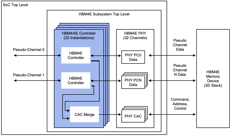
HBM4E Memory Subsystem
HBM is a high-performance memory standard that features reduced power consumption and a small form factor. It combines a 2.5D/3D architecture with a wider interface at a lower clock speed (as compared to GDDR) to deliver higher overall throughput at a higher bandwidth-per-watt efficiency for AI/ML and high-performance computing (HPC) applications.
Rambus HBM memory controllers support data rates up to 16 Gb/s per data pin (HBM4E) and can be paired with 3rd-party or customer PHY solutions.
Controller
- Controller (source code)
- Testbench (source code)
- Complete documentation
Controller
- Expert technical support
- Maintenance updates
- Customization
- SoC Integration
Engineering Design Services:
- Package design
- System board layout
- Statistically-based signal and power integrity analysis
HBM4E Memory: Break Through to Greater Bandwidth

Delivering unrivaled memory bandwidth in a compact, high-capacity footprint, has made HBM the memory of choice for AI training. HBM4 is the fourth major generation of the HBM standard, with HBM4E offering an extended data rate and the same feature set. The Rambus HBM4E Controller provides industry-leading performance to 16 Gb/s, enabling a memory throughput of over 4 TB/s for training recommender systems, generative AI and other compute-intensive AI workloads.
Frequently Asked Questions about HBM
HBM is a high-performance memory standard that delivers extremely high bandwidth at excellent power efficiency by employing up to a 2048-bit wide interface.
HBM memory offers excellent bandwidth and capacity with superior power efficiency that makes it an ideal solution for AI/ML training workloads.
To achieve its high bandwidth, HBM uses a 2048-bit wide data interface in the latest generation HBM4/4E. This is far more than can be supported on a standard PCB used by traditional (2D) memory solutions. So, HBM employs a silicon interposer where traces can be very finely etched. This structure is called 2.5D. In addition, HBM uses 3D-stacked memory devices, giving HBM a 2.5D/3D architecture.
HBM memory is ideal for data-intensive applications like AI/ML, graphics, and HPC, where large amounts of data need to be processed at very high bandwidth.
HBM3E and GDDR6: Memory Solutions for AI

AI/ML changes everything, impacting every industry and touching the lives of everyone. With AI training sets growing at a pace of 10X per year, memory bandwidth is a critical area of focus as we move into the next era of computing and enable this continued growth. AI training and inference have unique feature requirements that can be served by tailored memory solutions. Learn how HBM3E and GDDR6 provide the high performance demanded by the next wave of AI applications.


