At Rambus, we create cutting-edge semiconductor and IP products, providing industry-leading chips and silicon IP to make data faster and safer.
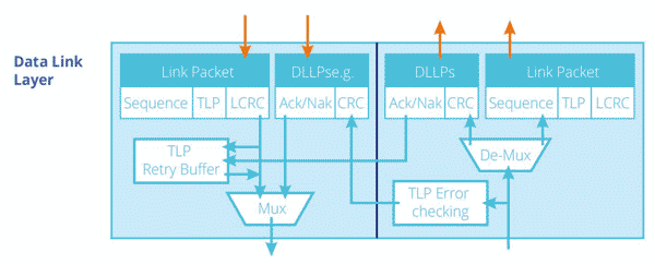
Data Link Layer
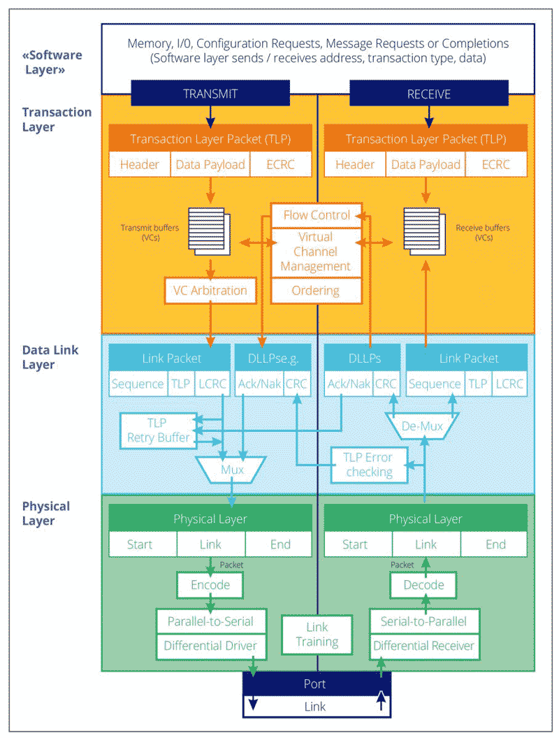
The Data Link Layer manages communication at the link level between the two connected PCIe components in order to ensure the correct transmission of packets. Its main roles are: generation and check of the CRC and Sequence Number of the TLP, initialization and update of flow control credits, generation of ACK/NAK, and the management of the Receive and Retry Buffers.
Deskew
The Deskew block in Rambus IP is a module located in Physical Layer that realigns data between lanes (misalignment can be due to lane-lane skew) and then identifies and sorts the packets according to type:
- PLP (Physical Layer Packets) are discarded
- DLLP (Data Link Layer Packets) are forwarded to the DLLP Decode block
- TLP (Transaction Layer Packets) are forwarded to the TLP Decode block
- The Deskew block is also responsible for detecting and reporting framing errors to the LTSSM and Configuration blocks
Device Readiness Notification
Allows a device to send a message to system to indicate when it is ready to accept first config access without sucessful status. Works with standard VDM; requires an extended capability for downstream ports. This feature helps avoid the long, architected, fixed delays following various forms of reset before software is permitted to perform its first Configuration Request. These delays can be very large:
- 1 second if Configuration Retry Status (CRS) is not used
- 100ms for most cases if CRS is used
- 10ms “minimum recovery time” when a Function is programmed from D3hot to D0
In addition, we avoid the complexity of using the existing CRS mechanism, which potentially requires polling periodically up to 1 second following reset by providing an explicit readiness indication.
DLCMSM
The DLCMSM (Data Link Control and Management State Machine) block implements the Data Link Control and Management State Machine. This state machine initializes the Data Link Layer to “dl_up” status, after having initialized Flow Control credits for Virtual Channel 0.
In order to do this, the DLCMSM:
- Is informed by the DLLP Decode block of the reception of Initialization Flow Control packets
- Orders the DLLP Encode block to transmit Initialization Flow Control packets
DLLP
Data Link Layer Packet. The DLLP Decode block checks and decodes the following types of DLLP:
- Initialization Flow Control DLLP: the DLLP Decode block informs the DLCMSM block of its reception and content
- Ack/Nak DLLP: the DLLP Decode block informs the TxSeqNum and CRC Generation of its reception and content so that the TLP contained in the Retry Buffer can be discarded or replayed
- Update Flow Control DLLP: the DLLP Decode block reports its content to the Tx Flow Control Credit block
- Power Management DLLP: the DLLP Decode block informs the Configuration block of its reception and content
The DLLP Encode block encodes the following different types of DLLP (Data Link Layer Packets):
- Initialization Flow Control DLLPs; when a request is received from the DLCMSM block
- High Priority Ack/Nak DLLPs; when the RxSeqNum and CRC Checking block reports that an incorrect TLP has been received, or when no Ack DLLP has been sent during a predefined time slot
- High Priority Update Flow Control DLLPs; based on the available Flow Control Credits reported by the Rx Flow Control Credit block
Power Management DLLPs; when a request is received from the Configuration block - Low Priority Update Flow Control DLLPs; based on the available Flow Control Credits reported by the Rx Flow Control Credit block
- Low Priority Ack/Nak DLLPs; based on the information reported by the RxSeqNum and CRC Checking block
- The encoded DLLPs are transmitted to the TxAlign and LTSTX block
If one or more DLLP is not acknowledged by the TxAlign and LTSTX block during a symbol time, the DLLP Encode block can change the DLLP content and its priority level to ensure that it always transmits the DLLP with the highest priority to the TxAlign and LTSTX block.
DMA
DMA (Direct Memory Access) is an efficient method of transferring data. A DMA engine handles the details of memory transfers to a peripheral on behalf of the processor, off-loading this task. A DMA transfer includes information about:
- Its source, which is defined by its interface, its transfer parameters and its starting address
- Its destination, also defined by its interface, parameters and address
- The DMAdTransfer configuration, which includes the transfer length (up to 4GB, but can be configured as infinite), its controls (start/end/ending criteria/interrupt/reporting request), and its status (error/end status/length)
Downstream Port
The port facing toward PCIe leaf segments (Upstream port or End Point).
DPA
DPA (Dynamic Power Allocation) extends existing PCIe device power management to provide active device power management substate for appropriate devices, while comprehending existing PCIe PM Capabilities including PCI-PM and Power Budgeting. An additional capability is implemented that contains advanced power allocations settings. This feature can be entirely implemented in application.
DPC
DPC (Downstream Port Containment) improves PCIe error containment and allows software to recover from async removal events that are not possible with the existing PCIe specification.
An Endpoint is a device that resides at the bottom of the branches of the tree topology and implements a single Upstream Port toward the Root. Native PCIe Endpoints are PCIe devices designed from scratch as opposed to adding a PCIe interface to old PCI device designs. Native PCIe Endpoints device are memory mapped devices (MMIO devices).
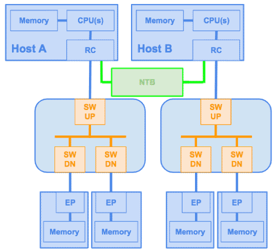
Non-Transparent Bridge (NTB)
A Switch is the PCIe component that allows to interconnect several PCIe devices. That is, it allows to extend the number of devices connected to the Host. PCIe Switch is transparent: all components in the PCIe hierarchy share the same address domain, defined by the (single) Host. In multiprocessor systems, each processor has its own address domain, defined during enumeration, and therefore can’t share the same address domain.
Non-Transparent Bridge (NTB) has two main purposes:
- allow inter-processor communication between different Hosts.
- ensure address domain isolation (by being non-transparent).
Being non-transparent, by definition, implies that one Host can’t enumerate or access directly other Host PCIe hierarchy.
Normal Mode
Normal mode is the default receive interface mode that is suitable for most applications with minimum complexity. In this mode:
- The Receive buffer is completely implemented inside the Core and is large enough to store all received TLPs
- All credit updates are handled internally
- Only TLPs intended for the user application are output on the Receive interface, in the order they are received from the link
Normal Mode with Non-Posted Buffer is similar to normal mode except that an additional buffer is implemented inside the Core that can be used to temporarily store non-posted TLPs. This enables the application to continue receiving posted and completion TLPs even when it is not ready to process non-posted TLPs.
NVMe
Specification that uses PCIe to provide the bandwidth needed for SSD applications.
Parity
Parity data protection is an optional feature that adds parity bits to data to protect it between the data link layer and the application’s logic.
PASID
PASID (Process Address Space ID) is an optional feature that enables sharing of a single Endpoint device across multiple processes while providing each process a complete 64-bit virtual address space. In practice this feature adds support for a TLP prefix that contains a 20 bit address space that can be added to memory transaction TLPs.
PCI Express Layer
The PCI Express layer consists of:
- a PCIe Controller
- a PCIe Tx/Rx Interface between the Bridge and the PCIe Controller
- a PCIe Configuration Interface to give the Bridge access to the PCIe Config Space
- a PCIe Misc Interface to allow the Bridge to manage Low-Power, Interrupts, etc.
PCIe Switch
A PCI Express switch is a device that allows expansion of PCI Express hierarchy. A switch device comprises one switch upstream, one or more switch downstream ports, and switching logic that routes TLPs between the ports. A PCI Express switch is “transparent”, meaning that software and other devices do not need to be aware of its presence in the hierarchy, and also there is no driver required to operate it.
Peer-to-Peer
In PCI Express, data transfers usually occurs only between the Root Complex and the PCI Express devices. However, peer-to-peer allows a PCI Express device to communicate with another PCI Express device in the hierarchy. In order for this to happen, Root-Ports and Switches must support peer-to-peer, which is optional.
Per-Vector Masking
Per-vector masking is an optional feature set by the Core Variable K_PCICONF that adds Mask Bits and Pending Bits registers to MSIcapability.
The Mask Bits register is programmed by the host and its value can be read by the application via the APB configuration interface, if required.
The behavior of the Pending Bits register depends on the associated interrupt:
- If an MSI is requested by the application and the corresponding message number is masked, then the Core sets the matching pending bit
- If an MSI is requested by the application and the corresponding message number is not masked, then the Core clears the matching pending bit
- If the interrupt request is satisfied while the interrupt source is still masked, then the application must write 1 to the corresponding bit through the APB configuration interface to clear it
PHYMAC
The PHYMAC (Physical Media Access Controller) Layer manages the initialization of the PCI Express link as well as the physical events that occur during normal operation. This layer functions at the PIPE clock frequency. The PHYMAC Layer consists of:
- The LTSSM block, which is the central intelligence of the physical layer
- On the receive side, one Deskew FIFO and eight similar RxLane blocks
- On the transmit side, one TxAlign and LTSTX block and eight TxLane blocks
Physical Functions (PFs)
Physical Functions (PFs) are full-featured PCIe functions; they are discovered, managed, and manipulated like any other PCIe device and PFs have full configuration space. It is possible to configure or control the PCIe device via the PF and in turn, the PF has the complete ability to move data in and out of the device. Each PCI Express device can have from one (1) and up to eight (8) physical PFs. Each PF is independent and is seen by software as a separate PCI Express device, which allows several devices in the same chip and makes software development easier and less costly.
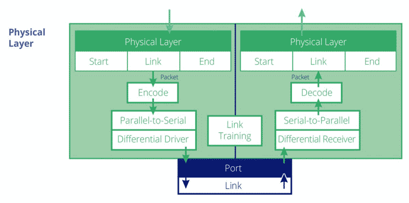
Physical Layer
The Physical Layer is the lowest hierarchical layer for PCIe as shown in the figure below. TLP and DLLP packets are sent from the Data Link Layer to the Physical Layer for transmission over the link. The Physical Layer is divided into 2 languages: the logical one and the electrical one. The Logical Physical Layer contains the digital logic that prepares the packets for serial transmission on the Link and reversing that process for inbound packets. The electrical Physical Layer is the analog interface of the Physical Layer that connects to the Link and consists of differential drivers and receivers for each lane.
PMUX
PMUX (Protocol Multiplexing) enables multiple protocols to share a PCIe Link. It is the mechanism to enable transmission of packets other than TLP/DLLP across the PCIe link.
Power Gating
Technique used to reduce power consumption when some blocks of a circuit are not in use. Power gating shuts off the current to prevent leakage currents.
PTM
PTM (Precision Time Measurement) enables the coordination of timing. It allows the transfer of information across multiple devices with independent local timebases without relying on software to coordinate time among all devices.
TLP Prefix
One or more DWORDs are pre-pend to TLP header in order to carry additional information for various purposes (TLP processing hints, PASID, MRIOV, vendor-specific..). TLP prefix support is optional and all devices from the requester to the completer must support this capability to be enabled.
TPH
Adding hints about how the system should handle TLPs targeting memory space can improve latency and traffic congestion. The spec defines TPH (TLP Processus Hint) as providing information about which of several possible cache locations in the system would be the optimal place for a temporary copy of a TLP. Enables a requester or completer (usually Endpoint) to set attributes in a request targetting system memory in order to help host optimize cache management. The mechanisms are used to:
- Ease the process of data residency/allocation within the hierarchy of system cache
- Reduce device memory access latencies and reduce statistical variation in latencies
- Minimize memory & system interconnect BW and its associated power consumption
- In addition, this information enables the Root Complex and Endpoint to optimize their handling of requests by identifying and separating data likely to be reused soon from bulk flows that could monopolize system resources. Providing information about expected data usage patterns allows the best use of system fabric resources such as memory, caches, and system interconnects, reducing possible limits on system performance.
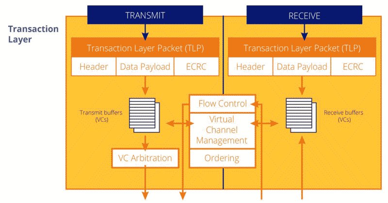
Transaction Layer
The Transaction Layer manages the generation of TLPs from both the Application Layer and the Configuration Space on the transmit side and checks for flow control credits before transmitting the TLPs to the Data Link Layer.
On the receive side, the transaction layer extracts received TLPs from the Receive buffer, checks their format and type, and then routes them to the Configuration Space or to the Application Layer. It also manages the calculation of credits for the Receive buffer. Even though it is not part of the Transaction Layer function, this layer also includes the Configuration Space, which can receive and generate dedicated TLP.