DDR4 Data Buffer
Home > Memory Interface Chips > DDR4 DIMM Chipset > DDR4 Data Buffer
Our DDR4 Data Buffer, acquired from Inphi, is built to deliver robust performance for real-time, memory-intensive applications, delivering leading I/O performance and margin. Compatible with DDR4 LRDIMMs, the Data Buffer is ideal for high-performance, high-capacity enterprise and data center systems.
How the DDR4 Data Buffer works
Increased memory capacity and performance are critical to solving today’s complex problems with huge data sets and accelerating Big Data applications.
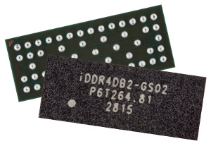
When combined with our DDR4 Register Clock Driver (RCD), iDDR4RCD-GS02, our DDR4 Data Buffer (DB), iDDR4DB2-GS02, recently acquired from Inphi, enables DDR4 Load Reduced Dual Inline Memory Modules (LRDIMMs) to deliver high-bandwidth performance with twice the capacity of DDR4 Registered DIMMs (RDIMMs).

Designed to meet the demanding requirements for real-time, memory-intensive applications, the DB delivers enhanced performance and margin at 2400 Mbps with built-in support for future data rates up to 2666 Mbps. This enables the highest speeds and robust operation when multiple LRDIMMs populate the memory channel for the highest system capacities.
The iDDR4DB2-GS02 dual 4-bit bidirectional data register with differential strobes is designed for 1.2 V VDD operation. The device has a dual 4-bit host bus interface that is connected to a memory controller and a dual 4-bit DRAM interface that is connected to two x4 DRAMs. It also has an input-only control bus interface that is connected to a DDR4 Register. This interface consists of a 4-bit control bus, two dedicated control signals, a voltage reference input and a differential clock input.
All DQ inputs are pseudo-differential with an internal voltage reference. All DQ outputs are VDD terminated drivers optimized to drive single or dual terminated traces in DDR4 LRDIMM applications. The differential DQS strobes are used to sample the DQ inputs and are regenerated in the DDR4 DB for driving out the DQ outputs on the opposite side of the device.
The clock inputs BCK_t and BCK_c are used to sample the control inputs BCOM[3:0], BCKE and BODT. The BCOM[3:0] inputs are used to write device internal control registers.
The iDDR4DB2-GS02 also supports dedicated pins for ZQ calibration and for parity error alerts.
Data Center Evolution: DDR5 DIMMs Advance Server Performance

Driven by a confluence of megatrends, global data traffic is increasing at an exponential rate. For example, 5G networks are enabling billions of AI-powered IoT devices untethered from wired networks. Nowhere is the impact of all this growth being felt more intensely than in data centers. Indeed, hyperscale data centers have become the critical hubs of the global data network. DDR5 DRAM will enable the next generation of server systems providing the massive computing power of hyperscale and enterprise data centers. Learn about the benefits of DDR5 memory and the design considerations for implementing DDR5 DIMMs.
Solution Offerings
- Meets or exceeds all JESD79-4 performance specifications for DDR4-2400 operation
- Pairs with RCD to be used in LRDIMM
- 2V Vdd supply
- Operational up to 2666 Mbps
- Advanced in-system debug capability
- Wide temperature range: -5° C – 125° C
- ROHS compliant
- High performance DDR4 servers
- High performance workstations
- High capacity storage systems
- High reliability & telecom systems
- DDR4 JEDEC standard LRDIMM designs, in conjunction with the DDR4 RCD, iDDR4RCD-GS02


