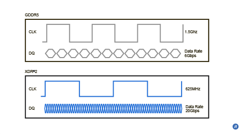
Rambus’ 32X Data Rate technology transfers 32-bits of data per I/O on every clock cycle. This enables extremely high bit-transfer rates and per device bandwidth while maintaining relatively low system clock speeds. Use of lower clock speeds reduces system costs and complexity.
- Reduces power consumption
- Simplifies design complexity
- Reduces board and system costs
- Enables high data rates while maintaining low-frequency system clock
What is 32X data rate technology?

Current industry standard memories employ double, or quad, data rate technology which transfers two, or four, bits of data per I/O for every clock cycle. Using quad data rate technology, GDDR5 memory requires a 1750 megahertz (MHz) clock to achieve a peak performance of 7 gigabits per second (Gbps) data rate and 28 gigabytes per second (GB/s) total bandwidth from a 4-byte wide device. The complexity and cost of routing, distributing and maintaining clock signals rise significantly as frequencies increase. This added cost and complexity reduces scalability.
32X Data Rate technology offers a scalable migration path to higher memory system performance and device bandwidth by enabling breakthrough signaling rates. A data rate of 20Gbps can be achieved with an easily manageable 625MHz system clock. This provides a total bandwidth of 80GB/s from a single 4-byte wide DRAM device.
Who Benefits?
By maintaining a low-frequency clock, memory system designers are able to achieve higher data rates without adding additional time, cost and complexity to the memory subsystem and board design and implementation. In addition, the low-speed clocks reduces the power consumption of the system. This translates to an overall improved time-to-market and reduced system cost.
