[Updated on March 4, 2026] In an era where data-intensive applications, from AI and machine learning to high-performance computing (HPC) and gaming, are pushing the limits of traditional memory architectures, High Bandwidth Memory (HBM) has emerged as a high-performance, power-efficient solution. As industries demand faster, higher throughput processing, understanding HBM’s architecture, benefits, and evolving role in next-gen systems is essential.
In this blog, we’ll explore how HBM works, how it compares to previous generations, and why it’s becoming the cornerstone of next-generation computing.
Table of Contents:
-
- What is High Bandwidth Memory (HBM) and How is it Reshaping the Future of Computing?
- What is 2.5D/3D Architecture?
- How is HBM4E / HBM4 Different from HBM3E, HBM3, HBM3, HBM2 or HBM (Gen 1)?
- What are the Additional Features of HBM4E / HBM4?
- Rambus HBM Memory Controller Cores for AI and High-Performance Workloads
- Summary
What is High Bandwidth Memory (HBM) and How is it Reshaping the Future of Computing?
As computing races toward higher speeds and greater efficiency, memory bandwidth has emerged as a major bottleneck for workloads like AI, high-performance computing, and data analytics. This is where High Bandwidth Memory (HBM) comes in. HBM is a cutting-edge 2.5D and 3D memory architecture designed with an exceptionally wide data path, enabling massive throughput and performance gains. Unlike traditional memory architectures that rely on horizontal layouts and narrow interfaces, HBM takes a vertical approach: stacking memory dies atop one another and connecting through through-silicon vias (TSVs). This 3D-stacked design drastically shortens data travel paths, enabling bandwidth and lower power consumption in a compact footprint.
HBM operates at incredible multi-gigabit speeds. When you combine that speed with a very wide data path, the result is staggering bandwidth, often measured in hundreds of Gigabytes per second (Gb/s) and even reaching into the Terabytes per second (TB/s) range.
To put this into perspective, an HBM4E device running at 16 GB/s delivers 4.096 TB/s of bandwidth. That level of performance is what makes HBM4E a leading choice for AI training hardware.
What is a 2.5D/3D Architecture?
2.5D and 3D architectures refer to advanced integration techniques that improve performance, bandwidth, and power efficiency by bringing components closer together—literally.
3D Architecture
The “3D” part is easy to see. In 3D architecture, chips are stacked vertically and connected through TSVs (vertical electrical connections that pass through the silicon dies). An HBM memory device is a packaged 3D stack of DRAM, forming a compact, high-performance memory module. Think of it as a high-rise building of chips with elevators (TSVs) connecting the floors.
2.5D Architecture
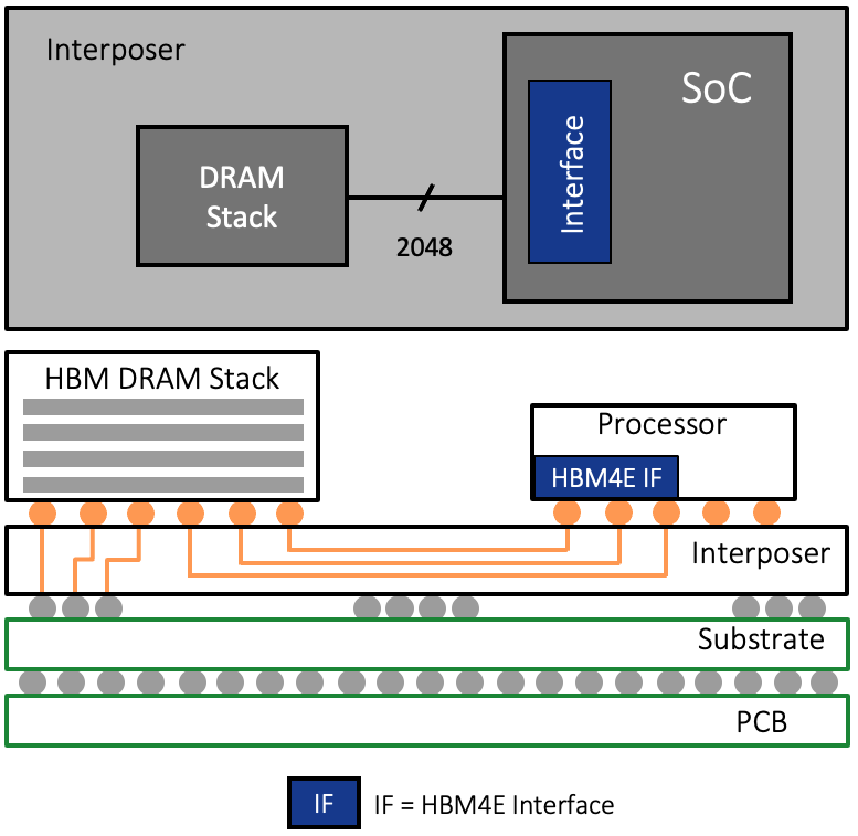
In a 2.5D setup, multiple chips, like a CPU, GPU, and in our case, HBM devices stacks are placed side-by-side on a silicon interposer – a thin substrate of silicon that acts as a high-speed communication bridge. The interposer contains the fine-pitch wiring that enables fast, low-latency connections between the chips.
Why do we need to use a silicon interposer? The data path between each HBM4E / HBM4 memory device and the processor requires 2,048 “wires” or traces. With the addition of command and address, clocks, etc. the number of traces necessary grows to about 3,000.
Thousands of traces are far more than can be supported on a standard PCB. Therefore, a silicon interposer is used as an intermediary to connect memory device(s) and processor. As with an integrated circuit, finely spaced traces can be etched in the silicon interposer enabling the desired number of wires needed for the HBM interface. The HBM device(s) and the processor are mounted atop the interposer in what is referred to as a 2.5D architecture.
HBM uses both 2.5D and 3D architectures described above, so it’s a 2.5D/3D architecture memory solution.
How is HBM4E / HBM4 Different from HBM3E, HBM3, HBM3, HBM2 or HBM (Gen 1)?
HBM4 represents a significant leap forward from its predecessors—HBM3E, HBM3 and earlier generations—in terms of bandwidth, capacity, efficiency and architectural innovation. With each generation, we’ve seen an upward trend in data rate, 3D-stack height, and DRAM chip density. That translates to higher bandwidth and greater device capacity with each upgrade of the specification.
When HBM launched, it started with a 1 Gb/s data rate and a 1024-bit wide interface. HBM delivered 128 GB/s of bandwidth, a huge step forward at the time. Since then, every generation has pushed the limits a little further. HBM2, HBM3, and now HBM3E have all scaled bandwidth primarily by increasing the data rate. For example, HBM3E runs at 9.6 Gb/s, enabling a 1229 GB/s of bandwidth per stack.
That’s impressive, but HBM4 took things to an entirely new level. HBM4 doubled the interface width from 1024 bits to 2048 bits. This architectural shift means that even at a modest 8 Gb/s data rate, HBM4 can deliver 2.048 TB/s of bandwidth per stack. That’s nearly double what HBM3E offers. HBM4E doubles the data rate to 16 Gb/s, which translates to an awesome bandwidth of 4.096 TB/s per attached HBM4E device.
Chip architects aren’t stopping at one stack. In fact, they’re designing systems with higher attach rates to feed the insatiable appetite of AI accelerators and next-gen GPUs. Imagine a configuration with eight HBM4E stacks, each running at 16 Gb/s. The result? A staggering 32.768 TB/s of memory bandwidth. That’s the kind of state-of-the-art throughput needed for massive AI models and high-performance computing workloads.
This table below shares the key differences between HBM4E / HBM4 and earlier generations.
| Generation | Data Rate (Gb/s) | Interface Width (b) | Bandwidth per Device (GB/s) | Stack Height | Max. DRAM Capacity (Gb) | Max. Device Capacity (GB) |
|---|---|---|---|---|---|---|
| HBM | 1.0 | 1024 | 128 | 8 | 16 | 16 |
| HBM2 | 2.0 | 1024 | 256 | 8 | 16 | 16 |
| HBM2E | 3.6 | 1024 | 461 | 12 | 24 | 36 |
| HBM3 | 6.4 | 1024 | 819 | 16 | 32 | 64 |
| HBM3E | 9.6 | 1024 | 1229 | 16 | 32 | 64 |
| HBM4 | 8.0 | 2048 | 2048 | 16 | 32 | 64 |
| HBM4E | 16.0 | 2048 | 4096 | 16 | 32 | 64 |
What are the Additional Features of HBM4E / HBM4?
But that’s not all. HBM4 introduced enhancements in power, memory access and RAS and these are inherited by HBM4E.
-
- Double the Memory Channels: HBM4 doubled the number of independent channels per stack to 32 with 2 pseudo-channels per channel. This provides designers more flexibility in accessing the DRAM devices in the stack.
- Improved Power Efficiency: HBM4 supports VDDQ options of 0.7V, 0.75V, 0.8V or 0.9V and VDDC of 1.0V or 1.05V. The lower voltage levels improve power efficiency.
- Compatibility and Flexibility: The HBM4 / HBM4E interface standard ensures backwards compatibility with existing HBM3 controllers, allowing for seamless integration and flexibility in various applications.
- Directed Refresh Management (DRFM): HBM4 / HBM4E incorporates Directed Refresh Management (DRFM) for improved Reliability, Availability, and Serviceability (RAS) including improved row-hammer mitigation.
Rambus HBM Memory Controller Cores for AI and High-Performance Workloads
Rambus delivers a comprehensive portfolio of HBM controller cores engineered for maximum speed and efficiency. Designed for high bandwidth and ultra-low latency, these controllers enable cutting-edge performance for AI training, machine learning, and advanced computing applications.
The lineup includes our industry-leading HBM4E memory controller, supporting data rates up to 16 Gb/s and offering exceptional flexibility for next-generation workloads. With Rambus HBM controllers, designers can achieve superior throughput, scalability, and reliability for demanding AI and HPC environments.
Summary
As computing demands continue to skyrocket, HBM stands out as a transformative technology that addresses the critical bottleneck of memory bandwidth. By leveraging advanced 2.5D and 3D architectures, HBM delivers massive throughput, exceptional power efficiency, and scalability for next-generation workloads. With HBM4E doubling the data rate to 16 Gb/s and carrying forward HBM4’s features for flexibility and reliability, it is poised to become the backbone of AI, HPC, and data-intensive applications. Understanding this evolution is key to achieving the performance required for tomorrow’s most demanding systems.
Explore more resources:
– HBM4E Memory: Break Through to Greater Bandwidth
– Unleashing the Performance of AI Training with HBM4
– Ask the Experts: HBM4 Memory Interface IP
Leave a Reply