• Skip to primary navigation
  • Skip to main content
  • Skip to footer
  • English
  • Investor Relations
  • Resource Library
  • Newsroom
  • Blog
  • Careers
  • Support Center
Rambus Logo

Rambus

At Rambus, we create cutting-edge semiconductor and IP products, spanning memory and interfaces to security, smart sensors and lighting.

  • Products
      • All
          • Memory Interface Chips
          • DIMM Chipsets
          • DDR5 DIMM Chipset
          • DDR4 NVRCD
          • DDR4 Register Clock Driver
          • DDR4 Data Buffer
          • CXL Memory Interconnect Initiative
          • Interface IP
          • Memory PHYs
          • GDDR6 PHY
          • HBM3 PHY
          • HBM2E PHY
          • DDR4 PHY
          • More…
          • SerDes PHYs
          • PCIe 6.0 PHY
          • PCIe 5.0 PHY
          • 32G C2C PHY
          • 32G PHY
          • 28G PHY
          • More…
          • Digital Controllers
          • Memory Controllers
          • CXL & PCI Express Controllers
          • MIPI Controllers
          • Video Compression and Forward Error Correction Cores
          • Security IP
          • Root of Trust Solutions
          • Security Protocol Engines
          • Inline Cipher Engines
          • Crypto Accelerator Cores
          • DPA Countermeasures
          • Software Protocols & Crypto Toolkits
          • Anti-Counterfeiting
          • Provisioning and Key Management
      • Memory Interface Chips
        • DIMM Chipsets
          • DDR5 DIMM Chipset
          • Non-Volatile DDR4 Registering Clock Driver
          • DDR4 Register Clock Driver
          • DDR4 Data Buffer
          • DDR3 Register Clock Driver
          • DDR3 Isolation Memory Buffer
        • CXL Memory Interconnect Initiative

        • Made for high speed, reliability and power efficiency, our DDR3, DDR4, and DDR5 DIMM chipsets deliver top-of-the-line performance and capacity for the next wave of computing systems. Learn more about our Memory Interface Chip solutions
      • Interface IP
          • Memory PHYs
            • GDDR6 PHY
            • HBM3 PHY
            • HBM2E PHY
            • DDR4 PHY
            • DDR4 Multi-modal PHY
            • DDR3 PHY
          • SerDes PHYs
            • PCIe 6.0 PHY
            • PCIe 5.0 PHY
            • PCIe 4.0 PHY
            • 32G C2C PHY
            • 32G PHY
            • 28G PHY
            • 16G PHY
            • 12G PHY
            • 6G PHY
          • Digital Controllers
            • HBM3 Controller
            • HBM2E Controller
            • GDDR6 Controller
            • LPDDR5 Controller
            • CXL 2.0 Controller
            • PCIe 6.0 Controller
            • PCIe 5.0 Controller
            • MIPI CSI-2/DSI-2 Controllers
            • Video Compression and Forward Error Correction Cores
            • More…

        • With their reduced power consumption and industry-leading data rates, our line-up of memory interface IP solutions support a broad range of industry standards with improved margin and flexibility. Learn more about our Interface IP solutions
      • Security IP
          • Root of Trust Solutions
          • Security Protocol Engines
            • MACsec Engines
            • IPsec, TLS, SSL Multi-Protocol Engines
            • High Speed Public Key Accelerator
          • Inline Cipher Engines
          • Crypto Accelerator Cores
            • DPA Resistant Cores
            • Basic Crypto Blocks
          • Anti-Counterfeiting
            • CryptoFirewall Cores
            • Circuit Camouflage Technology
          • DPA Countermeasures
            • DPA Resistant Cores
            • DPA Resistant Software Libraries
            • DPA Workstation Platform
          • Software Protocols & Crypto Toolkits
            • IPsec Toolkit
            • FIPs Cryptographic Libraries
            • MACsec Toolkit
            • IoT Security Framework
          • CryptoMedia
            • Content Protection Core
            • Content Protection Services
          • Provisioning and Key Management
            • CryptoManager Provisioning
            • CryptoManager Device Key Management

        • From chip-to-cloud-to-crowd, Rambus secure silicon IP helps protect the world’s most valuable resource: data. Securing electronic systems at their hardware foundation, our embedded security solutions span areas including root of trust, tamper resistance, content protection and trusted provisioning. Learn more about our Security IP offerings
  • Markets
      • AI & Machine Learning
        • Speed and Security for the Artificial Intelligence & Machine Learning Revolution
          • Products
          • SerDes PHYs
          • Memory PHYs
          • Digital Controllers
          • Memory Interface Chips
          • Root of Trust
          • Crypto Accelerator Cores
          • Protocol Engines
          • Provisioning and Key Management
          • AI & Machine Learning
      • Automotive
        • Providing Performance & Security for the Connected Car
          • Products
          • Memory PHYs
          • SerDes PHYs
          • Digital Controllers
          • Root of Trust
          • PKE Engine
          • MACsec Engines
          • Crypto Accelerator Cores
          • Provisioning and Key Management
          • Explore Automotive
      • Data Center
        • Optimizing capacity, connectivity and capability of the cloud
          • Products
          • SerDes PHYs
          • Memory PHYs
          • Digital Controllers
          • Memory Interface Chips
          • Root of Trust
          • MACsec Engines
          • Software Protocols
          • Provisioning and Key Management
          • See Data Center
      • Edge
        • Catching a tidal wave of data
          • Products
          • Memory PHYs
          • SerDes PHYs
          • Digital Controllers
          • Root of Trust
          • Crypto Accelerator Cores
          • Protocol Engines
          • Software Protocols
          • Discover Edge
      • Government
        • Securing Mission-critical Systems
          • Products
          • Root of Trust
          • Protocol Engines
          • Anti-Tamper Cores
          • Provisioning and Key Management
          • DPA Workstation Platform
          • SerDes PHYs
          • Memory PHYs
          • Digital Controllers
          • See Government
      • IoT
        • Making IoT Data Safe & Fast
          • Products
          • Root of Trust
          • TLS Toolkits
          • Provisioning and Key Management
          • Memory PHYs
          • SerDes PHYs
          • Digital Controllers
          • Explore IoT
  • Resources
    • Inventions
    • Buying Guide
    • Resource Library
      • Webinars
      • Product Selector
  • About
      • Corporate Overview
      • Leadership
      • Inventors
      • Careers
      • Locations
      • Investor Relations
      • Newsroom
      • Blog
      • Events
      • Partnerships
      • Certifications
      • Corporate Responsibility
      • Contact
Home > Inventions > Memory + Interfaces > DLL/PLL on a DRAM

DLL/PLL on a DRAM

As CPU speeds continue to increase, memory performance becomes more of a limiting factor in system performance. For system performance to increase, memory performance must increase as well. An important aspect of increasing memory performance is increasing the speed at which data can be transmitted to and from the DRAMs in the memory system. In the early 1990s, Rambus designed the first DRAMs that incorporated DLLs and PLLs, important innovations that allowed DRAMs to achieve 500 MHz signaling rates, more than eight times faster than the prevailing DRAM communication rates at the time.

  • Maximizes operating frequency of a memory system
  • Increases DRAM performance
  • Improves DRAM yield and reduced production costs

What is DLL/PLL on a DRAM Technology?

Low and high-speed signaling without a DLL/PLL on a DRAM

Modern systems use synchronous communication to achieve high data transmission rates to and from the DRAMs in the memory system. Systems that communicate synchronously use a clock signal as a timing reference so that data can be transmitted and received with a known relationship to this reference. A difficulty in maintaining this relationship is that process, voltage, and temperature variations can alter the timing relationship between the clock and data signals, resulting in reduced timing margins. This problem gets worse as signaling speeds increase, limiting the ability of systems to communicate data at higher speeds.

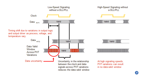
Timing margins, in particular, can be affected by process, voltage, and temperature at low and high signaling speeds. At low signaling speeds (the left side of Figure 1), DataPVT1 illustrates the relationship of the data valid window (the time over which data can be reliably sampled by the receiver) and the clock for a given set of operating conditions. Likewise, DataPVT2 shows the relationship of the data valid window and the clock for a different set of operating conditions. These two sets of operating conditions represent the operational extremes over which the device functions. Receiver circuitry does not typically understand how the data valid window changes as process, voltage, and temperature change at the transmitter. Because of this, the receiver circuitry is designed to sample data within a window of time that data is valid across all allowed operating conditions. If DataPVT1 and DataPVT2 represent the soonest and latest (relative to the clock signal) data valid windows, then the receiver will assume a data valid window that is the intersection of these two, and choose a sample point within this resulting data valid window that is valid across process, voltage, and temperature variations.

At low signaling speeds, the data valid window (the time over which data can be sampled reliably by the receiver) can be large. Even in the presence of a substantial shift in the data valid window across operational extremes, the resulting data valid window can still be large enough to transmit and receive data reliably. This is the case for DRAM technologies such as SDRAM. However, for higher-speed DRAM technologies such as RDRAM and DDR, variations in process, voltage, and temperature can result in the loss of the data valid window. The right side of Figure 1 shows that at higher signaling speeds, the data valid windows for both DataPVT1 and DataPVT2 are smaller, reflecting the fact that information must be transmitted more quickly at higher signaling rates. Although the data valid windows are smaller, these windows still shift the same amount across process, voltage, and temperature (assuming no manufacturing improvements or changes in operating environment). Because these data valid windows are smaller, the resulting intersection of the data valid windows yields no resulting data valid window during which receiver circuitry can reliably sample data.

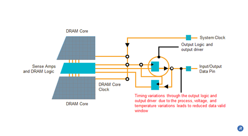
As process, voltage, and temperature vary, the timing characteristics of the output logic and output driver change, causing the data valid window to shift. In order to transmit and receive data at high speeds, this timing variation needs to be addressed.

DLL/PLL on a DRAM block diagram

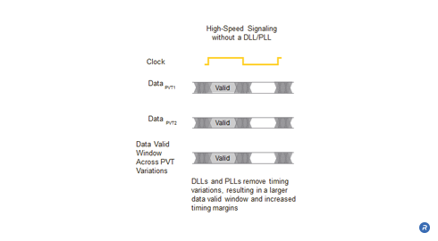
Delay Lock Loops (DLLs) and Phase Lock Loops (PLLs) serve similar purposes, and can be used to maintain a fixed timing relationship between signals in environments where process, voltage, and temperature variations cause these relationships to change over time. DLLs and PLLs work by continuously comparing the relationship between two signals and providing feedback to adjust and maintain a fixed relationship between them. Rambus DRAMs were the first DRAMs to incorporate DLLs and PLLs, an important innovation that resulted in increased signaling speeds, compared to alternative DRAM technologies.

Maintaining timing with a DLL/PLL on a DRAM

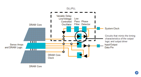
A DLL is used to maintain the timing relationship between a clock signal and an output data signal. A critical element of the DLL is the phase detector, which detects phase differences between the clock and output data. The phase detector detects this phase difference, and sends control information through a low pass filter to a variable delay line that adjusts the timing of the internal clock to maintain the desired timing relationship (PLLs use a voltage controlled oscillator to adjust this timing relationship). One of the difficulties of maintaining phase relationships between these two signals is that the loop which provides feedback to the phase detector must account for the timing characteristics of the output logic and output driver. This is important, as it estimates the phase differences between the clock and the data being driven by the output driver. In order to accomplish this, circuits that mimic the behavioral characteristics of the output logic and output driver are inserted into this feedback loop to model timing delays and changes in behavior as process, voltage, and temperature vary. Maintaining the timing relationships between the clock and output data in this manner with DLLs and PLLs results in improved timing margins (as shown in Figure 4), and addresses an important limitation to increasing signaling speeds.

PLLs are similar to DLLs, but can also be used to divide-down or multiply-up an external system clock frequency for use in other parts of a chip. PLLs can be used to provide a slower clock frequency to the core of a DRAM, while the interface operates at a higher clock frequency. PLLs used in this manner enable DRAM core prefetch, allowing the DRAM core to operate at a slower frequency (improving DRAM yield), while allowing the interface to run at higher speeds to improve system performance.

High-speed signaling with a DLL/PLL on a DRAM

In 1993 Rambus published details of a 500 MHz PLL design at the International Solid State Circuits Conference (ISSCC), the premier conference on circuit design. One year later, Rambus published details of a 500 MHz DLL in a paper presented at ISSCC in 1994. Both papers received prestigious Best Paper awards in recognition of the groundbreaking innovations described in each.

Who Benefits?

End Users, DRAM manufacturers, designers and integrators can all benefit by incorporating a DLL/PLL on a DRAM. By providing a fixed timing relationship between clock and data signals, DRAM performance is allowed to increase and end users are able to benefit from the overall improvement in system performance. DRAM manufactures are able to reduce production costs and improve DRAM yields with the ability to adjust the timing relationships to compensate for variations in process, voltage and temperature, improving timing margins. By enabling high per-pin transfer rates, DLLs and PLLs allow controller and board designers to reduce IO pin counts, which decreases packaging costs, component count, routing area, and routing complexity. Finally, the ability of DLLs and PLLs to provide fixed timing relationships lets component manufacturers and system integrators relax the specifications. In systems with varying temperature and voltage characteristics, system thermal and power delivery requirements can be relaxed and the DRAMs can still maintain good timing margins, while lowering the costs of the thermal solution, power supply, and system manufacturing.

Footer

About

  • Corporate Overview
  • Leadership
  • Careers
  • Locations
  • Investor Relations
  • News
  • Corporate Responsibility

Products

  • Memory PHYs
  • SerDes PHYs
  • Digital Controllers
  • Server DIMM Chipsets
  • Root of Trust Solutions
  • Provisioning and Key Management
  • Protocol Engines
  • Crypto Accelerator Cores
  • Software Protocols
  • DPA Countermeasures
  • Anti-Counterfeiting
  • CryptoMedia

Markets

  • AI & Machine Learning
  • Automotive
  • Data Center
  • Edge
  • Government
  • IoT
  • Pay TV

Resources

  • Resource Library
  • Webinars
  • Inventions
  • Buying Guide
  • Contact

Copyright © 2023 Rambus.com. All Rights Reserved. Privacy Policy | Trademark & Guidelines

  • Facebook icon
  • Twitter icon
  • YouTuve icon
  • LinkedIn icon
  • Blog icon