• Skip to primary navigation
  • Skip to main content
  • Skip to footer
  • enEnglish
  • Investor Relations
  • Resource Library
  • Newsroom
  • Blog
  • Careers
  • Support Center
Rambus Logo

Rambus

At Rambus, we create cutting-edge semiconductor and IP products, spanning memory and interfaces to security, smart sensors and lighting.

  • Products
      • All
          • Interface IP
          • Memory PHYs
          • GDDR6 PHY
          • HBM2E PHY
          • DDR4 PHY
          • More…
          • SerDes PHYs
          • PCIe 5.0 PHY
          • PCIe 4.0 PHY
          • 112G LR PHY
          • 112G XSR PHY
          • 56G PHY
          • 32G PHY
          • 28G PHY
          • More…
          • Northwest Logic Controllers
          • Memory Controllers
          • PCI Express Controllers
          • MIPI Controllers
          • Security IP
          • Root of Trust Solutions
          • Provisioning and Key Management
          • CryptoManager Provisioning
          • CryptoManager Device Key Management
          • Protocol Engines
          • MACsec Engines
          • Multi-Protocol Engines
          • Crypto Accelerator Cores
          • DPA Resistant Cores
          • Basic Crypto Blocks
          • DPA Countermeasures
          • Software Protocols & Crypto Toolkits
          • Anti-Counterfeiting
          • Memory Interface Chips
          • Server DIMM Chipsets
          • DDR5 DIMM Chipset
          • DDR4 NVRCD
          • DDR4 Register Clock Driver
          • DDR4 Data Buffer
          • More…
      • Interface IP
          • Memory PHYs
            • GDDR6 PHY
            • HBM2E PHY
            • DDR4 PHY
            • DDR4 Multi-modal PHY
            • DDR3 PHY
          • SerDes PHYs
            • PCIe 5.0 PHY
            • PCIe 4.0 PHY
            • 112G LR PHY
            • 112G XSR PHY
            • 56G PHY
            • 32G PHY
            • 28G PHY
            • 16G PHY
            • 12G PHY
            • 6G PHY
          • Northwest Logic Controllers
            • PCIe 5.0 Controller
            • PCIe 4.0 Controller
            • HBM2E Controller
            • GDDR6 Controller
            • LPDDR4 Controller
            • DDR4 Controller
            • DDR3 Controller
            • MIPI DSI-2 Controller Core
            • MIPI CSI-2 Controller Core

        • With their reduced power consumption and industry-leading data rates, our line-up of memory interface IP solutions support a broad range of industry standards with improved margin and flexibility. Learn more about our Interface IP solutions
      • Security IP
          • Root of Trust
          • Provisioning and Key Management
            • CryptoManager Provisioning
            • CryptoManager Device Key Management
            • Secure Silicon Provisioning
            • Secure Device Provisioning
          • Protocol Engines
            • MACsec Engines
            • Multi-Protocol Engines for IPsec, TLS and SSL
            • High Speed Public Key Accelerator
          • Crypto Accelerator Cores
            • DPA Resistant Cores
            • Basic Crypto Blocks
          • Anti-Counterfeiting
            • CryptoFirewall Cores
            • Circuit Camouflage Technology
          • DPA Countermeasures
            • DPA Resistant Cores
            • DPA Resistant Software Libraries
            • DPA Workstation Platform
          • Software Protocols & Crypto Toolkits
            • Cloud-optimized IPsec Toolkit
            • Secure Communication Toolkits
            • IoT Security Framework
          • CryptoMedia
            • Content Protection Core
            • Content Protection Services

        • From chip-to-cloud-to-crowd, Rambus secure silicon IP helps protect the world’s most valuable resource: data. Securing electronic systems at their hardware foundation, our embedded security solutions span areas including root of trust, tamper resistance, content protection and trusted provisioning. Learn more about our Security IP offerings
      • Memory Interface Chips
        • Server DIMM Chipsets
          • DDR5 DIMM Chipset
          • Non-Volatile DDR4 Registering Clock Driver
          • DDR4 Register Clock Driver
          • DDR4 Data Buffer
          • DDR3 Register Clock Driver
          • DDR3 Isolation Memory Buffer

        • Made for high speed, reliability and power efficiency, our DDR3, DDR4, and DDR5 chipsets for RDIMM and LRDIMM server modules deliver top-of-the-line performance and capacity for the next wave of enterprise and data center servers. Learn more about our Memory Interface Chip solutions
  • Markets
      • AI & Machine Learning
        • Speed and Security for the Artificial Intelligence & Machine Learning Revolution
          • Products
          • SerDes PHYs
          • Memory PHYs
          • Digital Controllers
          • Memory Interface Chips
          • Root of Trust
          • Crypto Accelerator Cores
          • Protocol Engines
          • Provisioning and Key Management
          • AI & Machine Learning
      • Automotive
        • Providing Performance & Security for the Connected Car
          • Products
          • Memory PHYs
          • SerDes PHYs
          • Digital Controllers
          • Root of Trust
          • PKE Engine
          • MACsec Engines
          • Crypto Accelerator Cores
          • Provisioning and Key Management
          • Explore Automotive
      • Data Center
        • Optimizing capacity, connectivity and capability of the cloud
          • Products
          • SerDes PHYs
          • Memory PHYs
          • Digital Controllers
          • Memory Interface Chips
          • Root of Trust
          • MACsec Engines
          • Software Protocols
          • Provisioning and Key Management
          • See Data Center
      • Edge
        • Catching a tidal wave of data
          • Products
          • Memory PHYs
          • SerDes PHYs
          • Digital Controllers
          • Root of Trust
          • Crypto Accelerator Cores
          • Protocol Engines
          • Software Protocols
          • Discover Edge
      • Government
        • Securing Mission-critical Systems
          • Products
          • Root of Trust
          • Protocol Engines
          • Anti-Tamper Cores
          • Provisioning and Key Management
          • DPA Workstation Platform
          • SerDes PHYs
          • Memory PHYs
          • Digital Controllers
          • See Government
      • IoT
        • Making IoT Data Safe & Fast
          • Products
          • Root of Trust
          • TLS Toolkits
          • Provisioning and Key Management
          • Memory PHYs
          • SerDes PHYs
          • Digital Controllers
          • Explore IoT
  • Resources
    • Inventions
    • Buying Guide
    • Resource Library
      • Webinars
  • About
      • Corporate Overview
      • Leadership
      • Inventors
      • Careers
      • Locations
      • Investor Relations
      • Newsroom
      • Blog
      • Events
      • Partnerships
      • Corporate Social Responsibility
      • Contact
Home > Inventions > Memory + Interfaces > Fly-by Command Address

Fly-by Command Address

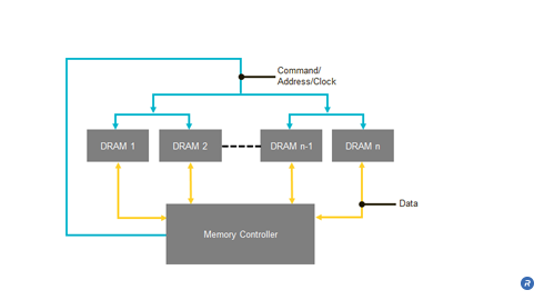
Conventional, low-speed DRAM systems distribute clock, command, and address signals to multiple DRAMs using a topology in which those signals propagate to all of the DRAMs in the system at approximately the same time. In such systems, the propagation delays on the command and address lines introduce timing skew into the system, thereby limiting the operating frequency of the bus and ultimately impacting the performance of high speed memory systems. In addition, the performance of these topologies is also limited by capacitive loading. Both the flight time skew problem and the capacitive loading issues discussed above through the use of the Fly-by architecture. Fly-by command/address architectures improve signal integrity in memory systems, thus enabling higher per-pin bit rates and systems capable of GHz data rates while maintaining low latency, and avoiding the need for clock-encoding.

  • Improves signal integrity and overall system performance
  • Simplifies system design with relaxed timing constraints

What is Fly-by Command Address Technology?

Portion of the data eye taken up be the “flight-time skew”

Although the skew in the clock, command, and address arrival times at each DRAM is small, the skew becomes significant as clock frequencies continue to increase. In such systems, the frequency limitations on the Command /Address (C/A) bus that result from the skew become a limiting factor in trying to achieve reliable GHz-speed memory operation performance.

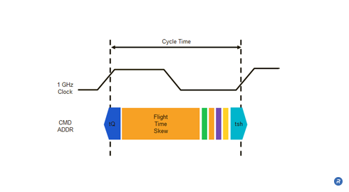
The variability in flight time from the memory controller to the memory devices, or “flight time skew”, can become a significant factor in high frequency systems with short clock periods. As shown, the flight time skew can consume a large portion of the available cycle time such that when operating at speeds greater than 1 GHz, very little time is left for reliable signal set-up and hold times. The issue is further compounded when operating at double data rates.

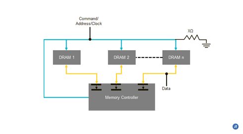
In trying to address the problem of flight time skew, a common solution is to try to match the trace lengths of the signal lines used to convey the command and address signals. One technique that tries to do such trace matching relies on a forked topology. In a forked topology, such as that illustrated below, the command, address, and clock signal traces are routed to a central node and then distributed from the central node to the individual DRAMs. By providing a signal distribution point closer to the DRAMs, the potential variability in trace length is limited to the shorter paths from the central node to the individual DRAMs.

Timing skew associated with a forked topology

Additionally, the performance of conventional DRAM topologies is constrained by capacitive loading. Adding memory devices to increase memory capacity on the module increases the capacitive loading of the C/A lines, thereby limiting the signaling rate on the C/A line.

Rambus patented innovations address both the flight time skew problem and the capacitive loading issues discussed above through the use of the Fly-by architecture. The Fly-by architecture was incorporated in Rambus DRAM systems as a means to enable increased memory capacity without impacting memory data rates. The Fly-by architecture optimizes the system transmission topology, is tolerant of timing skews and, when used in combination with FlexPhase™ circuit technology, can further manage any skew issues. Fly-by enables point-to-point data lines with scalable capacity without compromising memory data rates.

Timing skew addressed with Fly-by topology

In the Fly-by architecture the clock, address, and command are transmitted source synchronously to the DRAMs. As shown in the figure above, the clock signal propagates with the address and control information such that those signals arrive together at the interface of each DRAM. However, in this topology, the set of signals propagating on those lines arrives at each DRAM at a slightly different time. As can be seen from the illustration above, the signals will arrive at DRAM 1 shortly before DRAM 2 and so on. Because the arrival times of the signals at the DRAM interfaces are distributed in time, the time at which the signals encounter the input capacitance of each of the DRAMs is similarly distributed, thus reducing the capacitive loading issues discussed above. The reduced capacitive loading enhances the signal integrity and enables higher data rate signaling.

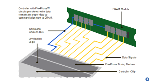
Further increases in data rates can be achieved by employing FlexPhase circuit technology to the data signals at the memory controller. Because the arrival times of the control and address signals at the DRAMs are distributed in time, the resulting data traffic received from the DRAMs on the separate data lines will also be slightly skewed in time. FlexPhase circuitry can be used to de-skew these incoming data signals. FlexPhase circuitry can also be used to pre-skew the data signals driven from the controller to the DRAMs so the data arrives with a well understood timing relationship with respect to the command and address signals.

The Fly-by Command Address architecture can also use routing traces on the circuit board that are terminated in order to achieve better controlled impedance on the line than would be realized using other topologies. Additional impedance mismatch reduction can be achieved by having shorter stub lengths from the command/address line to each DRAM device on the memory module. The improved impedance characteristics of the signal lines results in smaller signal reflections and less noise, which in turn enables higher frequency signaling.

Fly-by Command Address example - System employing Fly-by topology

In addition to providing higher data rates, another significant advantage of the Fly-by approach is that it is highly scalable in that multiple additional DRAMs can be inserted in a system to meet the needs of the relevant applications. With the added DRAMs, the Fly-by architecture is able to maintain high data rates on the Command/Address/Clock signals, whereas other topologies are limited by flight time skew, capacitive loading and impedance mismatches. Such non-Fly-by topologies often must reduce signaling rates on the Command/Address lines to accommodate the added DRAMs, thereby reducing system performance.

When used with FlexPhase circuit technology, the Fly-by architecture allows designers to relax PCB trace length requirements because the timing variations can be managed on the memory module with the FlexPhase circuit technology. Rambus has also developed Dynamic Point to Point technologies that, when used in combination with Fly-by, enable memory upgrades while maintaining bandwidth.

Who Benefits?

Fly-by architectures enable subsystems that require operational data rates that are significantly greater than those achievable with conventional approaches. Using Fly-by architectures allows designers to relax PCB trace length requirements allowing much simpler and more compact memory sub-system layouts.

In addition, Fly-by architectures provide system benefits by enabling DRAM systems to operate with GHz data rates. This superior DRAM system performance results in improved performance in desktops, notebooks, enterprise servers and storage, HDTVs, gaming systems, and handheld portable devices for end users.

Footer

About

  • Corporate Overview
  • Leadership
  • Careers
  • Locations
  • Investor Relations
  • News
  • Corporate Social Responsibility

Products

  • Memory PHYs
  • SerDes PHYs
  • Northwest Logic Controllers
  • Server DIMM Chipsets
  • Root of Trust Solutions
  • Provisioning and Key Management
  • Protocol Engines
  • Crypto Accelerator Cores
  • Software Protocols
  • DPA Countermeasures
  • Anti-Counterfeiting
  • CryptoMedia

Markets

  • AI & Machine Learning
  • Automotive
  • Data Center
  • Edge
  • Government
  • IoT
  • Pay TV

Resources

  • Resource Library
  • Webinars
  • Inventions
  • Buying Guide
  • Contact

Copyright © 2021 Rambus.com. All Rights Reserved. Privacy Policy | Trademark & Guidelines

  • Facebook icon
  • Twitter icon
  • YouTuve icon
  • LinkedIn icon
  • Blog icon