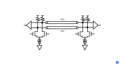
As data rates continue to increase, signal and power integrity are increasingly difficult to maintain in memory systems with single-ended signaling topologies. To enhance signal integrity and noise immunity across all communications between the memory PHY and the DRAM devices, Rambus implemented a Fully Differential Memory Architecture (FDMA) using a point-to-point topology, for data, clock, and command/address (C/A) channels. FDMA inherently reduces interference noise from simultaneous switching outputs (SSO) and crosstalk. Further, it reduces the EMI that would otherwise be generated in a single-ended system operating at the same data rate or frequency. With these advantages, FDMA enables very high-speed data transmission supported by full-speed operation of C/A channels.
- Enables low-power, high-performance memory systems
- Simplifies system design
- Increases system reliability through improved noise immunity
What is a Fully Differential Memory Architecture?

Differential signaling uses two wires for each signal (bit). A complementary signal is transmitted on one line or the other using a small DC current. The current is passed through a resistor on each line to generate a voltage, the difference being measured at the receiver. Depending on the polarity, the signal is interpreted as a “1” or “0”. SSO noise, a function of the cumulative value of the total amount of current change, is reduced because the same amount of current is generated regardless of the bit’s value.
A further advantage of differential signaling is that for a given voltage at the transmitter, twice the voltage difference is measured at the receiver (the difference in voltage between the two wires in the current loop). This compares with single-ended signaling that exhibits the same voltage at the transmitter and receiver (the difference between the voltage on the wire and ground). Twice the voltage at the receiver means it takes twice as much noise to exceed the threshold of a valid voltage level.
In addition, differential signaling has superior noise immunity when compared to single-ended signaling due to its inherent common mode noise rejection. Any voltage noise that couples into one wire of a pair is likely to couple into the other. Because the difference between the two signals is measured at the receiver, the common noise components are effectively cancelled out. In addition to being less susceptible to noise, differential signal pairs create less EMI than single-ended signals. This is because changes in signal level in the two wires create opposing electromagnetic fields that superimpose and cancel each other out, reducing crosstalk and spurious emissions.
Who Benefits?
FDMA offers a scalable architecture for delivering memory system bandwidth performance up to and beyond one terabyte per second. It supports a lower operating power at any given data rate since lower voltage levels than those required in a single-ended system can be used to maintain sufficient signal integrity. Further, FDMA simplifies overall system design and increases reliability by harnessing differential signaling advantages of superior noise immunity and lower EMI generation.
