At Rambus, we create cutting-edge semiconductor and IP products, providing industry-leading chips and silicon IP to make data faster and safer.
PCIe 5.0 Controller
Home > Interface IP > PCI Express Controller IP > PCIe 5.0 Controller
The Rambus PCIe 5.0 Controller (formerly XpressRICH from PLDA) is designed to achieve maximum PCI Express® (PCIe®) 5.0 performance with great design flexibility and ease of integration. It is fully backward compatible with PCIe 4.0 and 3.1/3.0. A PCIe 5.0 Controller with AXI (formerly XpressRICH-AXI) is also available. The controller delivers high-bandwidth and low-latency connectivity for next-generation applications in artificial intelligence/machine learning (AI/ML), data center, edge, 5G infrastructure and graphics.
 Contact
 PCIe 5.0 Controller
How the PCIe 5.0 Controller Works
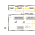
The PCIe 5.0 Controller is configurable and scalable IP designed for ASIC and FPGA implementation. It supports the PCIe 5.0, 4.0 and 3.1/3.0 specifications, as well as the version 5.x of the PHY Interface for PCI Express (PIPE) specification. The IP can be configured to support endpoint, root port, switch port, and dual-mode topologies, allowing for a variety of use models.
Rambus integrates and validates the PCIe 5.0 Controller with the customer’s choice of 3rd-party PCIe 5.0 PHY.
Data Center Evolution: The Leap to 64 GT/s Signaling with PCI Express 6.1

The PCI Express® (PCIe®) interface is the critical backbone that moves data at high bandwidth and low latency between various compute nodes such as CPUs, GPUs, FPGAs, and workload-specific accelerators. With the rapid rise in bandwidth demands of advanced workloads such as AI/ML training, PCIe 6.1 jumps signaling to 64 GT/s with some of the biggest changes yet in the standard.
Solution Offerings
PCIe 5.0 Controller
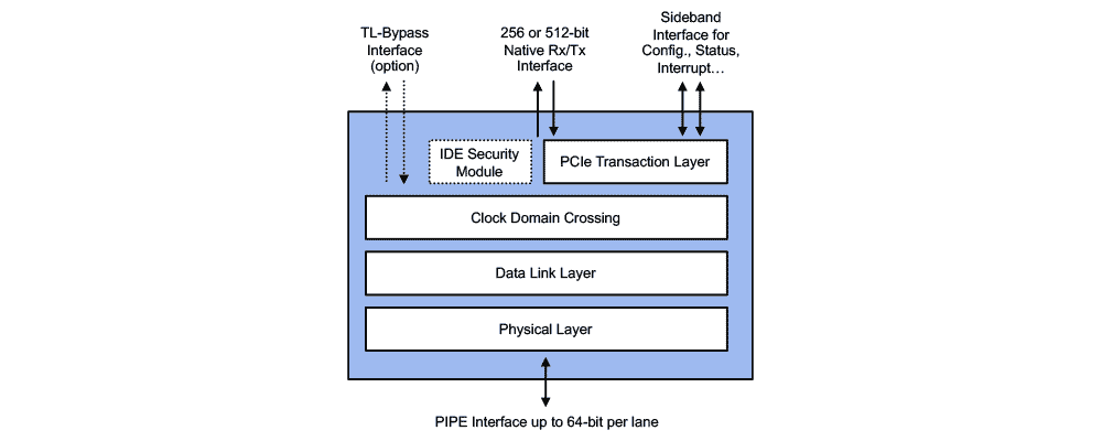
PCI Express layer- Comprises complete PCIe 5.0 interface subsystem with Rambus PCIe 5.0 PHY
- Supports the PCI Express 5.0 rev. 1.0 (32 GT/s), 4.0 (16 GT/s), 3.1/3.0 (8 GT/s), and PIPE 5.x (8, 16, 32 and 64-bit) specifications
- Compliant with PCI-SIG Single-Root I/O Virtualization (SR-IOV) Specification
- Supports Endpoint, Root-Port, Dual-mode, Switch port configurations
- Supports x16, x8, x4, x2, x1 at Gen5, Gen4, Gen3, Gen2, Gen1 speeds
- Supports up to 64 Physical Functions (PF), 512 Virtual Functions (VF)
- Supports AER, ECRC, ECC, MSI, MSI-X, Multi-function, crosslink, DOE, CMA over DOE, and other optional features and ECNs
- Additional optional features include OBFF, TPH, ARI, LTR, IDO, L1 PM substates, etc.
User Interface layer
- 512-bit or 256-bit transmit/receive low-latency user interface
- Up to 2 TLP per clock cycle in TLP Bypass mode (TLP chaining)
- User-selectable Transaction/Application Layer clock frequency
- Sideband signaling for PCIe configuration access, internal status monitoring, debug, and more
- Optional Transaction Layer bypass
Integrity and Data Encryption (IDE)
- Implements the PCI Express IDE ECN
- Configurable IDE engine
- Supports x1 to x16 lanes
- 256-bit or 512-bit data bus for PCIe IDE
- Configurable pipeline stages for difference process nodes for best cost and performance balance
- Supports containment and skid modes
- Supports multi-stream
- Utilizes high-performance AES-GCM for encryption, decryption, authentication
- PCIe IDE TLP aggregation for 1, 2, 4, 8 TLPs
- PCIe IDE automatic IDE prefix insertion and detection
- PCIe IDE automatic IDE sync/fail message generation
- PCRC calculation & validation
- Efficient key control/refresh
- Bypass mode
Unique Features & Capabilities
- Internal data path size automatically scales up or down (256, 512 bits) based on max. link speed and width for reduced gate count and optimal throughput
- Dynamically adjustable application layer frequency down to 8Mhz for increased power savings
- Optional MSI/MSI-X register remapping to memory for reduced gate count when SR-IOV is implemented
- Configurable pipelining enables full speed operation on Intel and Xilinx FPGA, full support for production FPGA designs (when supported)
- Ultra-low Transmit and Receive latency (excl. PHY)
- Smart buffer management on receive side (Rx Stream) allows implementation of custom credit management schemes in the application logic
- Merged Replay and Transmit buffer enables lower memory footprint
- Advanced Reliability, Availability, Serviceability (RAS) features include LTSSM timers override, ACK/NAK/Replay/UpdateFC timers override, unscrambled PIPE interface access, error injection on Rx and Tx paths, recovery detailed status and much more, allowing for safe and reliable deployment of IP in mission-critical SoCs
- Optional Transaction Layer bypass allows for customer specific transaction layer and application layer
- Optional QuickBoot mode allows for up to 4x faster link training, cutting system-level simulation time by 20%
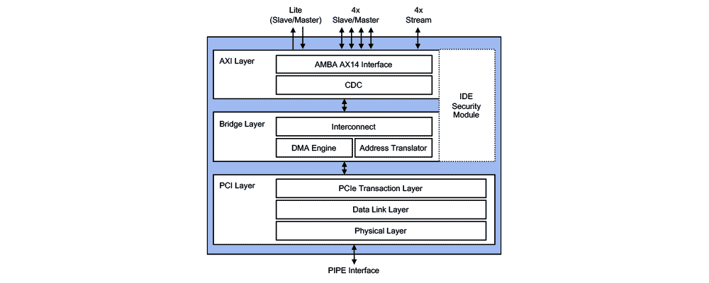
PCIe 5.0 Controller with AXI
PCI Express layer- Comprises complete PCIe 5.0 interface subsystem with Rambus PCIe 5.0 PHY
- Supports the PCI Express 5.0 rev. 1.0 (32 GT/s), 4.0 (16 GT/s), 3.1/3.0 (8 GT/s) and PIPE (8, 16, 32 and 64-bit) specifications
- Supports the PCI-SIG Single-Root I/O Virtualization (SR-IOV) Specification
- Supports Endpoint, Root-Port, Dual-mode configurations
- Supports x16, x8, x4, x2, x1 at Gen5, Gen4, Gen3, Gen2, Gen1 speeds
- Supports up to 64 Physical Functions (PF), 512 Virtual Functions (VF)
- Supports AER, ECRC, ECC, MSI, MSI-X, Multi-function, crosslink, DOE, CMA over DOE, and other optional features and ECNs
- Additional optional features include LTR, L1 PM substates, etc.
AMBA AXI layer
- Compliant with the AMBA® AXI™ Protocol Specification (AXI3, AXI4 and AXI4-Lite) and AMBA® 4 AXI4-Stream Protocol Specification
- Supports multiple, user-selectable AXI interfaces including AXI Master, AXI Slave, AXI Stream
- Each AXI interface data width independently configurable in 512-, 256-, 128-, and 64-bit
- Each AXI interface can operate in a separate clock domain
- Supported Burst types include INCR, FIXED, WRAP
- Narrow transfers supported
Integrity and Data Encryption (IDE)
- Implements the PCI Express IDE ECN
- Configurable IDE engine
- Supports x1 to x16 lanes
- 256-bit or 512-bit data bus for PCIe IDE
- Configurable pipeline stages for difference process nodes for best cost and performance balance
- Supports containment and skid modes
- Supports multi-stream
- Utilizes high-performance AES-GCM for encryption, decryption, authentication
- PCIe IDE TLP aggregation for 1, 2, 4, 8 TLPs
- PCIe IDE automatic IDE prefix insertion and detection
- PCIe IDE automatic IDE sync/fail message generation
- PCRC calculation & validation
- Efficient key control/refresh
- Bypass mode
Data engines
- Optional built-in Legacy DMA engine
- Up to 8 DMA channels, Scatter-Gather, descriptor prefetch
- Completion reordering, interrupt and descriptor reporting
- Optional Address Translation tables for direct PCIe to AXI and AXI to PCIe communication
Unique Features & Capabilities
- Internal data path size automatically scales up or down (64, 256, 512 bits) based on link max. speed and width for reduced gate count and optimal throughput
- Configurable pipelining enables full speed operation on Intel and Xilinx FPGA, full support for production FPGA designs up to Gen5x4/Gen4 x8/Gen3 x16 with same RTL code
- Stringent implementation of PCIe to AXI Ordering Rules and AXI to PCIe Ordering Rules guarantees AXI deadlock prevention
- Carefully engineered AXI bridge & AXI interconnect allows full performance on AXI interfaces
- Availability of multiple AXI Master interfaces, a key benefit for high end SSD to maximize throughput
- Advanced Reliability, Availability, Serviceability (RAS) features include LTSSM timers override, ACK/NAK/Replay/UpdateFC timers override, unscrambled PIPE interface access, error injection on Rx and Tx paths, recovery detailed status and much more, allowing for safe and reliable deployment of IP in mission-critical SoCs
- Optional QuickBoot mode allows for up to 4x faster link training, cutting system-level simulation time by 20%
IP files
- Verilog RTL source code
- Libraries for functional simulation
- Configuration assistant GUI
Documentation
PCI Express Bus Functional Model
- Encrypted Simulation libraries
Software
- PCI Express Windows x64 and Linux x64 device drivers
- PCIe C API
Reference Designs
- Synthesizable Verilog RTL source code
- Simulation environment and test scripts
- Synthesis project & DC constraint files (ASIC)
- Synthesis project & constraint files for supported FPGA hardware platforms (FPGA)\
Advanced Design Integration Services:
- Integration of commercial and proprietary PCIe PHY IP
- Development and validation of custom PCIe PCS layer
- Customization of the Controller IP to add customer-specific features
- Generation of custom reference designs
- Generation of custom verification environments
- Design/architecture review and consulting
Protocol Compatibility
| Protocol | Signaling Rate (GT/s) | Application |
|---|---|---|
| PCIe 3.1/3.0 | 8 | Servers, storage, networking devices |
| PCIe 4.0 | 16 | Servers, storage, networking devices |
| PCIe 5.0 | 32 | AI, servers, storage, networking, 5G infrastructure |


Inventions