Video: How SOCAMM2 Brings LPDDR Power Efficiency to Scalable AI Server Memory
As AI models grow larger and more power hungry, memory is emerging as a key limiter in AI server design. In this Ask the Experts video, Piero Bianco, Senior Director of Product Marketing for Power Management ICs at Rambus, explains how SOCAMM2 addresses the power, scalability, and serviceability challenges of modern AI servers.
Watch the video to learn how SOCAMM2 combines the bandwidth and power efficiency of LPDDR5X with the modularity and reliability required in data center environments.
What This Video Covers
In this Ask the Experts session, Rambus explores how SOCAMM2 enables next‑generation AI servers, including:
- Why memory power consumption is becoming a limiting factor for AI scaling
- How LPDDR differs from traditional DDR memory in AI workloads
- The challenges of soldered LPDDR in data center environments
- What SOCAMM2 is and how it works
- Key benefits of SOCAMM2 for AI server designers
- What Rambus provides in its SOCAMM2 server module chipset
Why Memory Power Matters for AI
The AI industry has made enormous advances in compute, GPUs, and accelerators. Today, power consumption is increasingly the limiting factor in scaling AI systems.
AI models require memory not only for capacity, but for constant, high‑bandwidth data movement. Moving weights, activations, and key‑value caches consumes significant energy. As models grow, memory power efficiency becomes as important as compute performance.
Why LPDDR Is Attractive for AI Workloads
LPDDR was originally designed for mobile devices, but its characteristics align well with AI requirements:
- High bandwidth
- Low signaling voltage
- Lower power consumption per bit transferred
For AI workloads that prioritize bandwidth and energy efficiency over ultra‑low latency, LPDDR offers clear advantages. However, LPDDR was designed to be soldered close to the processor, which creates challenges in server environments.
The Limitations of Soldered LPDDR in Servers
Using soldered LPDDR in AI servers introduces several operational challenges:
- Repairability: If a memory device fails, the entire board must be replaced
- Supply chain rigidity: Memory configuration is fixed at manufacturing time
- Lack of upgradability: Capacity cannot be expanded over the system’s lifetime
- Service costs: Repairs require more downtime and labor
These limitations reduce flexibility and increase total cost of ownership in data centers.
What Is SOCAMM2?
SOCAMM2 stands for Small Outline Compression Attached Memory Module. It is a JEDEC‑defined memory standard that uses LPDDR5X packaged into a compact, server‑grade module.
Instead of soldering LPDDR directly onto the board, SOCAMM2 places LPDDR memory on a removable module. The module is designed to preserve LPDDR’s low‑voltage signaling and power efficiency while enabling modularity and serviceability.
SOCAMM2 modules sit flat on the motherboard, maximizing signal integrity and supporting the physical and electrical constraints of AI server designs.
Key Benefits of SOCAMM2 for AI Servers
SOCAMM2 delivers a combination of benefits tailored to AI infrastructure:
High Bandwidth with Low Power
SOCAMM2 preserves LPDDR’s core advantages, delivering high bandwidth at significantly lower power consumption compared to traditional server memory.
Modularity and Serviceability
Failed memory modules can be replaced without swapping entire boards, reducing downtime and maintenance cost.
Scalability
SOCAMM2 allows memory to be placed farther from the CPU while maintaining signal integrity, enabling higher memory capacity configurations around AI processors.
Improved Cooling Options
The flat, compression‑attached form factor creates more spacing for airflow and liquid cooling, which is critical for high‑power AI systems.
Industry Standardization
As a JEDEC standard, SOCAMM2 enables multi‑vendor sourcing and avoids proprietary lock‑in for system designers and operators.
What Rambus Provides for SOCAMM2
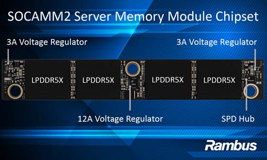
Rambus offers a complete SOCAMM2 server module chipset, designed to support enterprise‑grade AI deployments.
The Rambus SOCAMM2 chipset includes:
- High‑efficiency on‑module power management ICs
- Multiple voltage regulators optimized for LPDDR5X
- An SPD hub supporting configuration, presence detection, and telemetry
- Integrated temperature sensing for monitoring and reliability
Together, these components enable robust, energy‑efficient SOCAMM2 module designs.
Why Choose Rambus for SOCAMM2 Chipsets?
Rambus brings decades of experience in high‑speed memory interfaces and system‑level design. Its deep expertise spans signal integrity, power conversion, noise reduction, and compact form factor memory systems.
By working closely with CPU vendors, memory suppliers, and system OEMs, Rambus helps customers deliver SOCAMM2 solutions with high reliability, efficient power delivery, and scalable performance for AI servers.
Frequently Asked Questions about SOCAMM2
What is SOCAMM2?
SOCAMM2 is a JEDEC‑standard memory module that packages LPDDR5X into a removable, server‑grade form factor for AI systems.
Why is SOCAMM2 important for AI servers?
It combines LPDDR’s power efficiency and bandwidth with the modularity, scalability, and serviceability required in data centers.
How is SOCAMM2 different from soldered LPDDR?
SOCAMM2 enables memory replacement, upgradeability, and better supply chain flexibility compared to soldered LPDDR designs.
What does Rambus supply for SOCAMM2?
Rambus provides a complete SOCAMM2 chipset including power management ICs and an SPD hub with telemetry support.

