Once targeted exclusively at GPUs, GDDR use cases are rapidly expanding beyond traditional GPU and graphic applications. This is primarily due to the demand for increased bandwidth across a diverse set of market verticals – including the data center and automotive sector. GGDR6 can help meet that demand.
Bandwidth and SI challenges
More specifically, DDR4 currently tops out at 3.2 Gb/s, while a maximum interface speed of 8 Gb/s is achievable with GDDR5. In contrast, GDDR6 devices will double interface speed to 16 Gb/s. Put simply, GDDR6 is expected to provide 5x the speed per pin of leading-edge DDR4, with the Rambus GDDR6 PHY supporting speeds up to 16Gbps per pin, across two 16bit channels to provide a maximum bandwidth of 512 Gbps (or 64GB/s).
With GDDR6 providing a maximum bandwidth of up to 64 GB/s, it is critical for ASIC designers to ensure that devices and systems aren’t affected by signal integrity issues. This is precisely why the Rambus GDDR6 PHY engineering team makes extensive use of modeling and simulation tools, as well as providing highly programmable circuits, debug interfaces and utilities. Moreover, our engineering team comprises a range of in-house experts that participate in all stages of the GDDR6 PHY design which will be available on leading FinFET process nodes. These include package and PCB design experts and layout gurus, as well as signal integrity and power integrity specialists.
The Rambus GDDR6 PHY IP Core
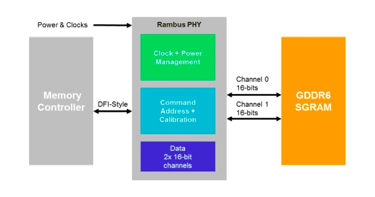
The JEDEC-compliant Rambus GDDR6 PHY IP Core will be optimized for systems that require low-latency and high-bandwidth GDDR6 memory solutions. The GDDR6 interface supports two independent channels, with each supporting 16 bits for a total data width of 32 bits. In addition, the PHY will be available on leading FinFET process nodes and support speeds up to 16Gbps per pin, providing a maximum bandwidth of up to 64 GB/s.
Delivered as a fully characterized hard macro, the Rambus GDDR6 PHY contains all of the necessary components for robust operation, including IO pads, PLL, clock distribution, transmit and receive paths, control logic, power distribution and electrostatic discharge (ESD) protection circuitry.
Additional GDDR6 PHY features will include 130um bump pitch; a 13/15-layer metal stack; a DFI-style interface for easy integration with the memory controller; support for Tx de-emphasis and Rx CTLE/DFE for channel optimization; selectable low-power operating states; programmable driver/termination impedance value; built-in test support (ATPG/boundary scans and IO Wrap loopback) and support for 2×16 clamshell mode (DRAM X8 mode enabled).
On the engineering side, the Rambus GDDR6 PHY will leverage our system-aware design methodology to facilitate flexible product integration. Specifically, we provide full system signal and power integrity analysis to optimize performance and chip layout. After a successful tapeout, GDDRY PHY customers receive a hard macro solution, along with a full suite of LabStation™ software that enables quick turn-on, characterization and debug. Moreover, the memory controller or PHY can be set as the ASIC interface master for training and calibrations (PHY independent mode).
Additional deliverables will include gate-level and IO models; a Verilog behavior model; layout abstracts (.lef); timing models (.lib); CDL netlists (.cdl); GDSII layout and DRC & LVS reports. The Rambus GDDR6 PHY is also packaged along with full documentation, such as datasheets, package design information, ASIC/DFT manufacturing guidelines, as well as a test and characterization user guide.
