Rambus will be showcasing a number of functional lensless smart sensor (LSS) prototypes at the CES 2016 PepCom Digital Experience tonight in Las Vegas. Developed in conjunction with frog design and IXDS, the prototypes include a drone (UAV), smartwatch as well as a maintenance and assembly platform.
Rambus showcases lensless smart sensor prototypes @ PepCom 2016
Reimagining the future of smart manufacturing
Written by Dr. Patrick Gill, Rambus Principal Research Scientist
From its inception, the Internet has been revolutionary in the way it moves data. Let’s explore what makes the Internet so effective, and determine if we can implement a similar revolution for physical goods manufacturing.
Rambus Renews Patent License Agreement with Toshiba
New agreement expands collaboration between companies to include a broad range of memory and interface technologies
SUNNYVALE, Calif. – December 28, 2015 – Rambus Inc. (NASDAQ:RMBS) today announced that it has renewed its patent license agreement with Toshiba Corporation. Under the terms of the new three-year agreement, Toshiba will be licensing a broad range of technologies from Rambus to cover products that include SoC’s with DRAM memory controllers and/or serial link interfaces, as well as Flash Memory and system products. Specific terms of this agreement are confidential.
“We are pleased to have expanded our relationship with Toshiba, one of the global leaders in the semiconductor industry,” said Luc Seraphin, senior vice president and general manager of the Memory and Interfaces Division at Rambus. “Toshiba has been a valuable customer of Rambus for more than a decade, and this renewal reinforces the value of our innovative technology and IP”.
Rambus develops enhanced, industry-compliant chipsets, custom memory and serial link technologies, and services to address power, performance, and capacity challenges for the mobile, connected device, and Big Data cloud computing markets. Rambus also drives innovations in silicon to cloud security and computational sensor technologies, making digital products safer and better.
For more details, please visit rambus.com
Follow Rambus
Company website: rambus.com
Rambus blog: rambusblog.com
Twitter: @rambusinc
LinkedIn: www.linkedin.com/company/rambus
Facebook: www.facebook.com/RambusInc
About Rambus Memory and Interfaces Division (MID)
The Rambus Memory and Interfaces Division develops products and services that solve the power, performance, and capacity challenges of the mobile, connected device, and cloud computing markets. Rambus enhanced standards-compatible and custom memory and serial link solutions include chips, architectures, memory and chip-to-chip interfaces, DRAM, IP validation tools, and system and IC design services. Developed through our system-aware design methodology, Rambus products deliver improved time-to-market and first-time-right quality.
About Rambus Inc.
Rambus creates cutting-edge semiconductor and IP products, spanning memory and interfaces to security, smart sensors and lighting. Our chips, customizable IP cores, architecture licenses, tools, services, training and innovations improve the competitive advantage of our customers. We collaborate with the industry, partnering with leading ASIC and SoC designers, foundries, IP developers, EDA companies and validation labs. Our products are integrated into tens of billions of devices and systems, powering and securing diverse applications, including Big Data, Internet of Things (IoT), mobile, consumer and media platforms. At Rambus, we are makers of better. For more information, visit rambus.com.
Rambus renews patent license agreement with Toshiba
Rambus has renewed its patent license agreement with Toshiba Corporation.
As per the terms of the new three-year agreement, Toshiba will be licensing a wide range of technologies from Rambus to cover products that include SoCs with DRAM memory controllers and/or serial link interfaces, as well as Flash Memory and system products.
Optimizing memory for next-gen computing
Semiconductor Engineering Editor in Chief Ed Sperling recently noted that getting data in and out of memory is just as important as optimizing the speed and efficiency of a processor.
“[Nevertheless], for years design teams managed to skirt the issue because it was quicker, easier and less expensive to boost processor clock frequencies with a brute-force approach,” he explained. “That worked well enough prior to 90nm, and adding more cores at lower clock speeds filled the gap starting at 65nm.”
Controllers Newsletter – Q4 2015
Northwest Logic Celebrates its 20th Anniversary
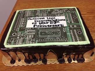
Northwest Logic was started in November of 1995 in the garage of one of the founding partners with an initial focus on providing FPGA-based design services. Over the years, we have grown into a provider of high-performance, high-quality IP Cores with a world-wide set of industry-leading customers. We want to thank all of our customers, partners, vendors and employees who been part of this journey. We look forward to continuing to work with you for another 20 years!
Thanks again, the Northwest Logic Team
Northwest Logic’s Memory Solution for 14nm Customers of Intel Custom Foundry
Northwest Logic’s DDR4/3 Controller Cores have been fully integrated and validated with Intel Custom Foundry’s DDR4/3 PHY. This complete solution is fully silicon-proven in a 14nm testchip. “With the successful integration of Northwest Logic’s DDR controller and Intel Custom Foundry’s DDR PHY IP, we now offer comprehensive DDR support to our customers”, said Tony Pialis, Director of Analog Mixed-Signal IP of Intel Custom Foundry. “Our customers can leverage the robust and silicon-ready IO solutions offered by Intel Custom Foundry and Northwest Logic.” Northwest Logic is one of the Intel Custom Foundry Eco-system partners. For more information, contact Northwest Logic or Intel.
CSI-2 Controller with C-PHY Support Released
Northwest Logic has released its CSI-2 Controller with full support of the MIPI C-PHY standard. The C-PHY uses 3-phase symbol encoding to carry data over 3 pins per lane (also known as trios). The C-PHY can support up to 3 trios at rates up to 2.5 Gsym/s for a peak bandwidth of 17.1 Gbit/s. This utilizes the same number of pins as a four lane D-PHY running at 2.5 Gbit/s/lane, but can carry 70% more data. The Northwest Logic CSI-2 Controller can support C-PHY, D-PHY and combo C/D-PHY. For this release, Northwest Logic delivered the controller integrated and verified with a combo C/D-PHY from Mixel. For more information, contact Northwest Logic.
Complete, Silicon-Proven PCI Express Solution
Northwest Logic provides a complete, silicon-proven, easy-to-use PCI Express solution for use in ASICs, Structured ASICs and FPGAs. The PCI Express and DMA IP cores have been used in a variety of designs including networking, storage, and military applications and on advanced process nodes including 16, 20, and 28 nm. For more information on this solution, please visit: www.nwlogic.com
DINI Group uses Northwest Logic’s PCI Express Solution to bring-up its ASIC Prototyping Platforms
DINI Group continues to use Northwest Logic’s PCI Express solution to bring up its ASIC prototyping platforms. The Kintex Ultrascale ASIC prototyping platform is one of their latest offerings. Visit DINI Group to see their complete selection of boards. “We have had very positive experience using Northwest’s IPs and we continue to use them for our ASIC board bring-up. We have been working with Northwest Logic for close to a decade now. They are our first choice for PCIe and memory interface IP,” said Mike Dini, President of DINI group. “DINI Group’s ASIC prototyping platforms, in combination with Northwest Logic’s silicon-proven PCI Express Cores, enable large PCIe-based designs to be quickly prototyped.”
MIPI D-PHY FPGA Prototyping Support from S2C
S2C’s MIPI D-PHY Interface Module provides both 4 channel MIPI D-PHY Rx and 4 channel MIPI D-PHY Tx support using the Meticom MC20901 Rx and MC20902 Tx chips. The list price of S2C Meticom MIPI D-PHY Interface Module (part number: P-MIPIPHYIB) is $400.00. Contact S2C for details.
Altia Systems Selects Northwest Logic’s MIPI Solution for its PanaCast 2 Video Camera
PanaCast 2 is the world’s first Panoramic-4K Plug-and-Play USB real time video camera that connects directly to your PC or Mac. It delivers a 180º wide by 54º tall panoramic video stream (3840X1080) and high fidelity stereo audio. “We use the Northwest Logic CSI-2 Rx Controller Core to bring MIPI data into the Xilinx Artix-7 FPGA inside our PanaCast 2 camera” said Yashket Gupta, Lead Engineer, Hardware Design. Adding, “We found the core easy to work with and support is top notch”. Please click here for more info in PanaCast 2. Please click here for more info on Northwest Logic MIPI Solutions.