Counterfeit chips, including gray market and rogue chips, have created an ongoing, multi-front battle for the semiconductor market to the tune of $75 billion annually, according to ResearchAndMarkets.com. The threat is more significant and broader than the chip maker’s bottom line. Counterfeit chips have numerous hidden dangers, including higher failure rates, corruption of data that can cause a system malfunction, exfiltration or stealing of proprietary information, and making systems vulnerable to cyberattacks. If we look at lessons from the past, the market could be at an elevated risk now.
Protecting against cybergeddon
Root of Trust CSDK Product Brief
Download the product brief to learn how the Root of Trust CSDK enables the rapid development of secure applications for the Root of Trust RT-600 series products.
Anti-Tamper Technologies
The design of chip anti-tamper protection needs to adapt and scale with rising threats. Adversaries range from high school hackers to well-funded state actors. Given the threats, it’s useful to think about anti-tamper countermeasures as a hierarchy of safeguards that parallel the type, effort and expense of attacks.
Rambus Delivers 112G XSR/USR PHY on TSMC 7nm Process for Chiplets and Co-Packaged Optics in Networking and Data Center
Highlights:
- Expands comprehensive portfolio of cutting-edge IP designed on TSMC’s industry-leading 7nm (N7) process
- Enables the most power- and cost-efficient solution for die-to-die (D2D) and die-to-optical engine (D2OE) connectivity over Extra Short Reach (XSR) and Ultra Short Reach (USR) channels
- Accelerates next-generation data center, networking, 5G, high-performance computing (HPC), and artificial intelligence/machine learning (AI/ML) applications with a critical building block enabling chiplet and co-packaged optics (CPO) architectures
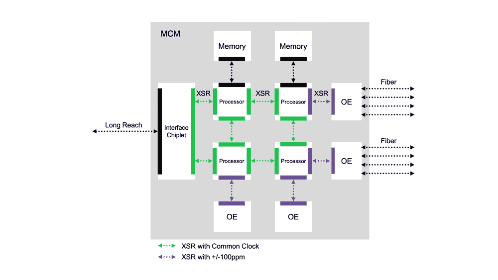
SUNNYVALE, Calif. – June 17, 2020 – Rambus Inc. (NASDAQ: RMBS), a premier silicon IP and chip provider making data faster and safer, today announced it has expanded its portfolio of high-speed interface IP on TSMC’s industry-leading 7nm process with the addition of its silicon-demonstrated 112G XSR/USR PHY. Offering unmatched power and area efficiency for next-generation applications, the 112G XSR/USR PHY is a critical enabler of chiplet and CPO architectures for data center, networking, 5G, HPC and AI/ML applications.
“Chiplets are already entering mainstream markets to enable cost-effective, high-performance products and to maintain signal integrity across variable physical distances,” said Shane Rau, research vice president, computing semiconductors at IDC. “SerDes PHYs at advanced process nodes, like the 7nm 112G XSR, enable that speed and signal integrity.”
The accelerated trend of disaggregation of large SoCs into multiple smaller chiplets demands faster time to market, yield improvement and design flexibility. The Rambus 112G XSR/USR PHY is a critical enabler of the D2D and D2OE interconnects for chiplet architectures. Implemented on TSMC’s advanced process technology, this chiplet connectivity solution has been demonstrated in silicon to exceed the challenging reach/BER performance of the CEI-112G XSR specification, and supports NRZ and PAM-4 signaling at various data rates for maximum design flexibility.
“We’re pleased with the availability of Rambus’ PHY on our N7 process technology to address the growing market need for low-power, high-performance chiplet architectures,” said Suk Lee, senior director of the Design Infrastructure Management Division at TSMC. “Our ongoing partnership with Rambus ensures that designers can meet next-generation requirements for performance and power efficiency in computing, AI/ML and networking using TSMC’s advanced process technologies.”
Leading-edge applications moving to chiplet architectures include next-generation 51.2 Terabit per second (Tbps) ASICs for network switches, where 112G XSR links will connect the digital switch ASIC die to CPO engines. In AI/ML and HPC SoCs, the 112G XSR PHY can be used to bridge purpose-built accelerator chiplets for natural language processing, video transcoding and image recognition. Another popular use case is the die disaggregation of large SoCs, hitting reticle size limits for manufacturable yields, into multiple smaller die connected using XSR links over organic substrate. Increasingly, these advanced applications are implemented on TSMC’s N7 process.
“This important milestone highlights Rambus’ leadership in high-speed SerDes enabling the industry’s highest value and most demanding applications,” said Hemant Dhulla, vice president and general manager of IP cores at Rambus. “At an industry-leading power efficiency of sub-picojoule per bit, and unidirectional bandwidth approaching two terabit per second per millimeter, we are very proud to offer our 112G XSR/USR solution in partnership with TSMC.”
Availability
The Rambus 112G XSR/USR PHY is available today for licensing and integrating into chiplet and SoC designs.
Additional Information
For additional details about the Rambus 112G XSR/USR PHY, please go to https://www.rambus.com/interface-ip/serdes/112g-xsr-phy/
Embedded Hardware Security Heads to the Edge
The days of building a moat around the castle to keep data secure were long gone before the pandemic led to a surge in remote work. With the enterprise network no longer rooted in a single place, every connection needs to be secured in line with increased server connectivity bandwidth requirements of cloud and edge computing.
Interview: NXP CEO Kurt Sievers | Cryptographers vs. Quantum Computers | The 8088
In this episode…Kurt Sievers is the new CEO of NXP, a job he’s been groomed for … for several years. We have an exclusive interview with Sievers, who discusses where NXP is going, and how he’s going to get it there. Also, quantum computing seems to threaten the very idea of cryptography. But that’s far from a guarantee. Today on the program we talk with Helena Handschuh from Rambus, who is one of the cryptography experts helping to devise algorithms to stand up against the most powerful computers man can conceive of.