Design complexity for advanced SoCs rises with each new process node, performance increase, and addition of new IP blocks. Designers are faced with increasing challenges to confidently verify and validate functionality of their chips. The LabStation Validation platform is a comprehensive tool suite for the rapid bring-up, validation and characterization of complex low-power, high-performance memory and serial link IP. It is designed to be easy to use and improve productivity while providing improved accuracy of test results and confidence is system performance.
LPDDR3 DRAM Product Brief
LPDDR3 PHY Product Brief
Fully compliant with LPDDR3 and LPDDR2 DRAM specifications, our LPDDR3 PHY pairs with the LPDDR3 DRAM to create a memory subsystem that supports data rates of up to 2133 Mbps, and reduces active memory system power by up to 25% and active DRAM power by up to 30%. This enables a significantly improved thermal profile and an increased battery life in the end device. The improved thermal profile also enables the memory system to run at peak bandwidth for longer periods of time, which translates to better overall performance in the end systems.
The improvement in power consumption is a result of Low Voltage Swing Terminated Logic (LVSTL), a single-ended, ground-terminated signaling technology, used while in R+ mode. LVSTL features a significantly reduced signal swing versus the 1.2 volt HSUL (High Speed Unterminated Logic) signal swing of standard LPDDR3. Reduced signal swing translates to significantly reduced IO power at high data rate, which is a major component of DRAM power. By supporting LVSTL and HSUL signaling, LPDDR3 offers a low-power mode while maintaining compatibility with LPDDR3 and LPDDR2 DRAM standards.
Phase Interpolator-Based CDR
In order to communicate data from one chip to another across a signal line, the receiving chip must know when to sample the data signal that it receives from the transmitting chip. In many systems, this information is provided by a timing (clock) signal sent from the transmitting chip to the receiving chip along a dedicated timing signal line adjacent to the data signal line. In systems with higher signaling rates, the receiving chip typically requires a clock alignment circuit, such as a Phase Locked Loop (PLL) or Delay Locked Loop (DLL), but the data timing must still be well-matched in order to eliminate timing skews. A phase interpolator based clock-data recovery circuit (CDR) is an alternative circuit architecture developed by Rambus which provides multiple advantages compared to PLL-based CDRs.
- Reduces cost, power and area of a CDR
- Improves jitter performance in high-speed links
What is Phase Interpolator-Based CDR Technology?
Buffered modules introduce a memory buffer between the memory controller and the DRAM devices on each module, isolating the DRAM from the memory bus and enabling an increase to the width of the memory without increasing the pin count of the controller. This also reduces the effective capacitive load on the memory bus enabling support for multiple modules at high speed.
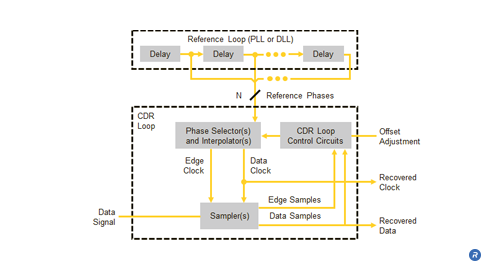
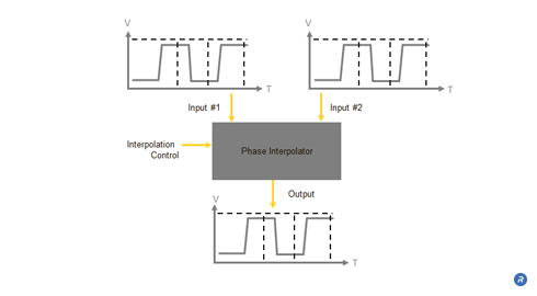
A phase-interpolator based CDR is an alternative circuit architecture developed by Rambus which provides multiple advantages compared to PLL-based CDRs. This type of CDR uses a PLL or DLL to implement a reference loop which accepts an input reference clock signal and produces a set of high speed clock signals, used as reference phases, spaced evenly across 360 degrees. These reference phases are then fed to a CDR loop which includes circuitry for selecting pairs of reference phases and interpolating between them to provide clocks for recovering the data from the data signal.
Because of the separation between the reference loop and the CDR loop, the designer of a phase interpolator based CDR can separately optimize both the noise suppression of the reference loop and the tracking agility of the CDR loop. Additionally, the reference loop is not affected by the contents of the data signal, potentially allowing this type of CDR to track a wider variety of data signals. Furthermore, the relatively long locking time of the reference loop applies only at start-up when initially locking to the reference clock signal. After the initial locking time, interpolator-based CDRs can provide much faster re-locking compared to PLL-based CDRs whenever the data signal returns after being interrupted.
Another benefit of phase interpolator based CDRs is that the data sampling point can be precisely adjusted by a digitally controlled offset. This allows the cancellation of offsets from device mismatches and other causes, and enables in-system measurements of the timing margin available for reliably extracting data from the data signal.
Lastly, although the reference loop can occupy the majority of the area and dissipate the majority of the power in a phase interpolator based CDR, its reference phases can be shared among several CDR loops on chips receiving multiple data signals. In this way, the average size and power required for the CDR functionality per data signal can be greatly reduced.
Who Benefits?
The use of phase interpolator based CDRs benefits many different groups. By designing ASICs including Rambus IO cells that utilize phase interpolator based CDRs, ASIC vendors benefit from the smaller area, lower power, and more stable operation of the IO cells. These benefits are magnified when dual, quad, or other multi-lane IO cells are used since these cells use one reference loop to drive multiple CDR loops for implementing multiple CDRs. The area and power savings can be significant compared to using a PLL per lane, as required by other CDR designs. The ability to digitally offset the data sampling clock when using a phase interpolator based CDR allows in-system testing of timing margins in the actual operating environment. Such system-level testing increases the reliability of manufactured systems for system integrators. Finally, the cost, power, performance, and testability benefits from using phase interpolator based CDRs is passed along to products purchased by consumers in the form of lower prices, longer battery life, and improved reliability.
Output Driver Calibration
Transmitting data at high speeds between a DRAM device and a memory controller requires careful design of IO drivers to ensure that the required electrical signaling levels are achieved. Variations in process, voltage, and temperature can alter the electrical characteristics of the output driver circuitry, resulting in deviations from the desired signaling levels. Additionally, variations in other system elements, such as trace impedance, reference voltage (Vref), and termination voltage (Vterm) can also impact signaling levels. To address these issues, Rambus pioneered the use of Output driver calibration in memory systems to improve communication speeds and provide greater reliability over a wide range of operating conditions.
- Improves data rates and system voltage margin
- Increases DRAM yield
- Compensates for variations in trace impedance and termination voltage
- Improves system reliability over a wide range of operating conditions
What is Output Driver Calibration Technology?
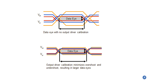
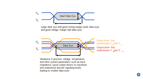
Variations in process, voltage, and temperature can reduce the size of data eyes. Data eyes reveal characteristics of the quality of the signaling environment such as timing and voltage margins. Robust signaling relies on having wide (good timing margin) and tall (good voltage margin) data eyes. Output drivers are designed to drive signals between high and low voltage levels, shown as Voh and Vol in the previous illustration. Variations in process, voltage, temperature, and other factors can cause output drivers to overshoot and/or undershoot the desired signaling voltage levels, resulting in reduced margins that impact signal integrity. Reduced timing margins limit the maximum signaling speed because the window of time over which the data is valid (width of the data eye) is smaller. Reduced voltage margins can require larger IO voltage swings to ensure accurate transmission of data, but such larger swings result in increased IO power and can increase the sensitivity of the system to cross talk. In order to increase signaling rates and reduce IO power, output driver overshoot and undershoot must be managed.
Output driver calibration allows for optimal signaling levels to be established and maintained using adjustable output drive strengths to compensate for variations in process, voltage, and temperature. Calibrating the output drivers during normal operation allows for drive strength adjustments to respond to changes in voltage and temperature which can fluctuate while a system is in use.
Output Driver Calibration uses feedback that is provided to the output driver circuitry to adjust the output impedance of the output driver circuitry, thereby controlling the circuit’s drive strength.in order to achieve optimal signal performance. The driver’s output impedance is compared to a reference resistor RZQ that is placed off the device. The output impedance is then calibrated to be equal to or proportional to the reference precision resistor.
The circuit above depicts how an Output Driver Calibration circuit may be configured. The voltage dropped across the topmost array of resistors is dependent upon the state of the respective transistors in series with those resistors and the value of the RZQ resistance on the line. The states of the transistors in the transistor array are individually controlled by the Drive Strength Register and are set so that the value of Vterm = Vref. The reference voltage, Vref , is representative of the desired output signal level. When the Vterm = Vref condition is achieved, the impedance in the top of the network divider is optimized for the driver. The values used for configuring the transistor array can be stored in the register and may be updated as needed.
The figure above illustrates the effect that Output Driver Calibration has on the magnitude of overshoot and undershoot along the transmission line. The reduction in overshoot and under-shoot results in increased voltage and timing margins.
The reference resistor RZQ and much of the circuitry for Output Driver Calibration can also be utilized for on-die termination ODT calibration.
Who Benefits?
Output driver calibration provides benefits from the device up through the system. By increasing DRAM yield and allowing DRAM output drivers to automatically compensate for process variation, output driver calibration improves margin and device testability, saving design and test time. Output driver calibration also allows board designers to compensate for variations in trace impedance and termination voltage caused by manufacturing and assembly processes. This ability to compensate for manufacturing tolerances of some components enables test specifications to be relaxed and saves component and tester costs.
At the system level, Output driver calibration enables system integrators to use one DRAM in multiple designs that utilize different trace impedances and that operate in different environments. Output driver calibration also increases voltage and timing margins, resulting in higher system reliability over a wider range of operating conditions. In addition, adjustable drive strengths help compensate for variations in temperature which allows system integrators to more effectively manage their system power and thermal budgets, thereby decreasing overall system cost.
Color Temperature Change
Since LEDs are available in a series of colors that cross the spectrum of white, there is a high degree of variation of color temperatures in lamps. This can make it difficult for consumers to blend new LED bulbs with existing lighting and can increase complexity of inventory management for professionals.
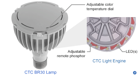
Rambus’ color temperature change (CTC) LED lamps can adjust from warm to neutral to cool with the simple turn of a dial – illuminating every application in its best light. This innovative technology cost effectively enables in-lamp color temperature change through the use of a remote phosphor and a color mixing light guide, without requiring additional LEDs or expensive multi-channel drivers.
Commercial Benefits
- Best price-performance
- Simplified SKU management
- Flexible and scalable to meet changing needs
Consumer Benefits
- Always achieve the look you want
- Tunable to match existing bulbs
- On-bulb dial for simple adjustment
What is Color Temperature Change Technology?
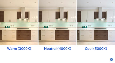
Rambus CTC technology uses a remote phosphor and a rotating color mixing light guide to continuously adjust the light output of the lamp from 5000 kelvin (K) to 3000K and all points in between. By turning a dial that controls the coverage amount of the remote phosphor, a user can control the amount of blue light emitted by the LEDs that is converted to amber, shifting the color temperature of the lamp. This technique enables the lamp to track along the black body curve and maintain a pure color temperature and high quality of light.
Who Benefits?
Consumers, store owners, distributors and facility managers alike benefit from the simple, cost-effective and flexible color temperate change technology that is integrated directly into the lamp. The Rambus in-lamp color adjustment technology allows the end user to continuously adjust color temperature to create the desired environment, from cool white of 5,000 kelvin to warm white of 3,000 kelvin, and all points in between. In the commercial sector, this technology enables simplified SKU management and is scalable to meet changing needs. Retailers need only one bulb on the store shelf to cover all the different color options that consumers require.