[Last updated on: January 23, 2024] In this blog post, we take an in-depth look at Compute Express Link®™ (CXL®™), an open standard cache-coherent interconnect between processors and accelerators, smart NICs, and memory devices.
- We explore how CXL can help data centers more efficiently handle the tremendous memory performance demands of generative AI and other advanced workloads.
- We discuss how CXL technology maintains memory coherency between the CPU memory space and memory on attached devices to enable resource sharing (or pooling).
- We also detail how CXL builds upon the physical and electrical interfaces of PCI Express® (PCIe®) with protocols that establish coherency, simplify the software stack, and maintain compatibility with existing standards.
- Lastly, we review Rambus CXL solutions, which include the Rambus CXL 3.1 Controller. This IP comes with integrated Integrity and Data Encryption (IDE) modules to monitor and protect against cyber and physical attacks on CXL and PCIe links.
Table of Contents
-
- Industry Landscape: Why Is a New Class of Interconnect Needed?
- An Introduction to CXL: What Is Compute Express Link?
- What Is the CXL Consortium?
- CXL Protocols & Standards
- Compute Express Link and PCIe: How Are They Related?
- CXL Features and Benefits
- CXL 2.0 and CXL 3.1 Features
- Rambus CXL Solutions
- Final Thoughts
1. Industry Landscape: Why is CXL needed?
Data centers face three major memory challenges as roadblocks to greater performance and lower total cost of ownership (TCO). The first of these is the limitations of the current server memory hierarchy. There is a three-order of magnitude latency gap that exists between direct-attached DRAM and Solid-State Drive (SSD) storage. When a processor runs out of capacity in direct-attached memory, it must go to SSD, which leaves the processor waiting. That waiting, or latency, has a dramatic negative impact on computing performance.
Secondly, core counts in multi-core processors are scaling far faster than main memory channels. This translates to processor cores beyond a certain number being starved for memory bandwidth, sub-optimizing the benefit of additional cores.
Finally, with the increasing move to accelerated computing, wherein accelerators have their own directed attached memory, there is the growing problem of underutilized or stranded memory resources.
Keep on reading:
– PCIe 6.1 – All you need to know
– CXL Memory Initiative: Enabling a New Era of Data Center Architecture
The solution to these data center memory challenges is a complimentary, pin-efficient memory technology that can provide more bandwidth and capacity to processors in a flexible manner. Compute Express Link (CXL) is the broadly supported industry standard solution that has been developed to provide low-latency, memory cache coherent links between processors, accelerators and memory devices.
2. An Introduction to CXL: What is Compute Express Link?
CXL is an open standard industry-supported cache-coherent interconnect for processors, memory expansion, and accelerators. Essentially, CXL technology maintains memory coherency between the CPU memory space and memory on attached devices. This enables resource sharing (or pooling) for higher performance, reduces software stack complexity, and lowers overall system cost. The CXL Consortium has identified three primary classes of devices that will employ the new interconnect:
-
-
- Type 1 Devices: Accelerators such as smart NICs typically lack local memory. Via CXL, these devices can communicate with the host processor’s DDR memory.
- Type 2 Devices: GPUs, ASICs, and FPGAs are all equipped with DDR or HBM memory and can use CXL to make the host processor’s memory locally available to the accelerator—and the accelerator’s memory locally available to the CPU. They are also co-located in the same cache coherent domain and help boost heterogeneous workloads.
- Type 3 Devices: Memory devices can be attached via CXL to provide additional bandwidth and capacity to host processors. The type of memory is independent of the host’s main memory.
-
3. What Is the CXL Consortium?
The CXL Consortium is an open industry standard group formed to develop technical specifications that facilitate breakthrough performance for emerging usage models while supporting an open ecosystem for data center accelerators and other high-speed enhancements.
4. CXL Protocols & Standards
The CXL standard supports a variety of use cases via three protocols: CXL.io, CXL.cache, and CXL.memory.
-
-
- CXL.io: This protocol is functionally equivalent to the PCIe protocol—and utilizes the broad industry adoption and familiarity of PCIe. As the foundational communication protocol, CXL.io is versatile and addresses a wide range of use cases.
- CXL.cache: This protocol, which is designed for more specific applications, enables accelerators to efficiently access and cache host memory for optimized performance.
- CXL.memory: This protocol enables a host, such as a processor, to access device-attached memory using load/store commands.
-
Together, these three protocols facilitate the coherent sharing of memory resources between computing devices, e.g., a CPU host and an AI accelerator. Essentially, this simplifies programming by enabling communication through shared memory. The protocols used to interconnect devices and hosts are as follows:
- Type 1 Devices: CXL.io + CXL.cache
- Type 2 Devices: CXL.io + CXL.cache + CXL.memory
- Type 3 Devices: CXL.io + CXL.memory
5. Compute Express Link vs PCIe: How Are They Related?
CXL builds upon the physical and electrical interfaces of PCIe with protocols that establish coherency, simplify the software stack, and maintain compatibility with existing standards. Specifically, CXL leverages a PCIe 5 feature that allows alternate protocols to use the physical PCIe layer. When a CXL-enabled accelerator is plugged into a x16 slot, the device negotiates with the host processor’s port at default PCI Express 1.0 transfer rates of 2.5 gigatransfers per second (GT/s). CXL transaction protocols are activated only if both sides support CXL. Otherwise, they operate as PCIe devices.
CXL 1.1 and 2.0 use the PCIe 5.0 physical layer, allowing data transfers at 32 GT/s, or up to 64 gigabytes per second (GB/s) in each direction over a 16-lane link.
CXL 3.1 uses the PCIe 6.1 physical layer to scale data transfers to 64 GT/s supporting up to 128 GB/s bi-directional communication over a x16 link.
6. CXL Features and Benefits
Streamlining and improving low-latency connectivity and memory coherency significantly bolsters computing performance and efficiency while lowering TCO. Moreover, CXL memory expansion capabilities enable additional capacity and bandwidth above and beyond the direct-attach DIMM slots in today’s servers. CXL makes it possible to add more memory to a CPU host processor through a CXL-attached device. When paired with persistent memory, the low-latency CXL link allows the CPU host to use this additional memory in conjunction with DRAM memory. The performance of high-capacity workloads depends on large memory capacities such as AI. Considering that these are the types of workloads most businesses and data-center operators are investing in, the advantages of CXL are clear.
7. CXL 2.0 and 3.1 Features
Memory Pooling
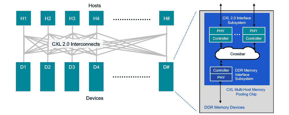
CXL 2.0 supports switching to enable memory pooling. With a CXL 2.0 switch, a host can access one or more devices from the pool. Although the hosts must be CXL 2.0-enabled to leverage this capability, the memory devices can be a mix of CXL 1.0, 1.1, and 2.0-enabled hardware. At 1.0/1.1, a device is limited to behaving as a single logical device accessible by only one host at a time. However, a 2.0 level device can be partitioned as multiple logical devices, allowing up to 16 hosts to simultaneously access different portions of the memory.
As an example, a host 1 (H1) can use half the memory in device 1 (D1) and a quarter of the memory in device 2 (D2) to finely match the memory requirements of its workload to the available capacity in the memory pool. The remaining capacity in devices D1 and D2 can be used by one or more of the other hosts up to a maximum of 16. Devices D3 and D4, CXL 1.0 and 1.1-enabled respectively, can be used by only one host at a time.
CXL 3.1 introduces peer-to-peer direct memory access and enhancements to memory pooling where multiple hosts can coherently share a memory space on a CXL 3.1 device. These features enable new use models and increased flexibility in data center architectures.
Switching
By moving to a CXL 2.0 direct-connect architecture, data centers can achieve the performance benefits of main memory expansion—and the efficiency and total cost of ownership (TCO) benefits of pooled memory. Assuming all hosts and devices are CXL 2.0 (and above)-enabled, “switching” is incorporated into the memory devices via a crossbar in the CXL memory pooling chip. This keeps latency low but requires a more powerful chip since it is now responsible for the control plane functionality performed by the switch. With low-latency direct connections, attached memory devices can employ DDR DRAM to provide expansion of host main memory. This can be done on a very flexible basis, as a host is able to access all—or portions of—the capacity of as many devices as needed to tackle a specific workload.
CXL 3.1 introduces multi-tiered switching which enables the implementation of switch fabrics. CXL 2.0 enabled a single layer of switching. With CXL 3.1, switch fabrics are enabled, where switches can connect to other switches, vastly increasing the scaling possibilities.
The “As Needed” Memory Paradigm
Analogous to ridesharing, CXL 2.0 and 3.1 allocate memory to hosts on an “as needed” basis, thereby delivering greater utilization and efficiency of memory. With CXL 3.1, memory pooling can be reconfigured dynamically without the need for a server (host) reboot. This architecture provides the option to provision server main memory for nominal workloads (rather than worst case), with the ability to access the pool when needed for high-capacity workloads and offering further benefits for TCO. Ultimately, the CXL memory pooling models can support the fundamental shift to server disaggregation and composability. In this paradigm, discrete units of compute, memory and storage can be composed on-demand to efficiently meet the needs of any workload.
Integrity and Data Encryption (IDE)
Disaggregation—or separating the components of server architectures—increases the attack surface. This is precisely why CXL includes a secure by design approach. Specifically, all three CXL protocols are secured via Integrity and Data Encryption (IDE) which provides confidentiality, integrity, and replay protection. IDE is implemented in hardware-level secure protocol engines instantiated in the CXL host and device chips to meet the high-speed data rate requirements of CXL without introducing additional latency. It should be noted that CXL chips and systems themselves require safeguards against tampering and cyberattacks. A hardware root of trust implemented in the CXL chips can provide this basis for security and support requirements for secure boot and secure firmware download.
Scaling Signaling to 64 GT/s
CXL 3.1 brings a step function increase in data rate of the standard. As mentioned earlier, CXL 1.1 and 2.0 use the PCIe 5.0 electricals for their physical layer: NRZ signaling at 32 GT/s. CXL 3.1 keeps that same philosophy of building on broadly adopted PCIe technology and extends it to the latest 6.1 version of the PCIe standard released in early 2022. That boosts CXL 3.1 data rates to 64 GT/s using PAM4 signaling. We cover the details of PAM4 signaling in PCIe 6 – All you need to know.
8. Rambus CXL Solutions
Rambus CXL 3.1 Controller
The Rambus CXL 3.1 Controller leverages the Rambus PCIe 6.1 Controller [link to https://www.rambus.com/interface-ip/pci-express/pcie6-controller/] architecture for the CXL.io protocol and adds the CXL.cache and CXL.mem protocols specific to CXL. The controller exposes a native Tx/Rx user interface for CXL.io traffic as well as an Intel CXL-cache/mem Protocol Interface (CPI) for CXL.mem and CXL. There is also a CXL 3.1 Controller with AXI version of the core that is compliant with the AMBA AXI Protocol Specification (AXI3, AXI4 and AXI4-Lite).
Read on:
– Rambus CXL Memory Initiative
– Rambus CXL & PCI Express Controllers
Zero-Latency IDE
The Rambus CXL 3.1 and PCIe 6.1 controllers are available with integrated Integrity and Data Encryption (IDE) modules. IDE monitors and protects against physical attacks on CXL and PCIe links. CXL requires extremely low latency to enable load-store memory architectures and cache-coherent links for its targeted use cases. This breakthrough controller with a zero-latency IDE delivers state-of-the-art security and performance at full 32 GT/s speed.
The built-in IDE modules employ a 256-bit AES-GCM (Advanced Encryption Standard, Galois/Counter Mode) symmetric-key cryptographic block cipher, helping chip designers and security architects to ensure confidentiality, integrity, and replay protection for traffic that travels over CXL and PCIe links. This secure functionality is especially imperative for data center computing applications including AI/ML and high-performance computing (HPC).
Key features include:
-
-
- IDE security with zero latency for CXL.mem and CXL.cache
- Robust protection from physical security attacks, minimizing the safety, financial, and brand reputation risks of a security breach
- IDE modules pre-integrated in Rambus CXL 3.1 and PCIe 6.1 controllers reduce implementation risks and speed time-to-market
-
Final Thoughts
CXL is a once-in-a-decade technological force that will transform data center architectures. Supported by a who’s who of industry players including hyperscalers, system OEMs, platform and module makers, chip makers and IP providers, its rapid development is a reflection of the tremendous value it can deliver.
This is why Rambus launched the CXL Memory Initiative—to research and develop solutions that enable a new era of data center performance and efficiency. Current Rambus CXL solutions include the Rambus CXL 3.1 Controller with integrated IDE.
Leave a Reply