In part one of this two-part series, Semiconductor Engineering Editor in Chief Ed Sperling and Rambus Sr. Director of Product Management Frank Ferro took a closer look at the various types of memory that system designers are using to support artificial intelligence (AI), machine learning (ML), and high-performance computing (HPC) applications. In this blog post, Sperling and Ferro explore how bandwidth-hungry AI/ML and HPC applications are driving new chip, system, and memory architectures.
“We’ve seen that HBM2 and HBM2E are frequently used in applications that demand high performance computing. These include AI/ML training in particular – along with certain networking applications that have locked in on HBM as a solution of choice,” Ferro confirms. “What is shipping out in the market today are solutions based on HBM2. HBM2 gives you a quite a bit of bandwidth. Although 2Gbps per pin isn’t very fast from a per pin standpoint, you’ve got 1024‑bit wide access, which gives you a total of 256 gigabytes of bandwidth.”
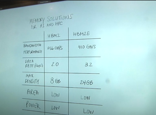
As Ferro notes, the 256Gbps represents the throughput that is delivered by HBM2.
“If you look at some of the applications in AI/ML training, if these are where you string multiple HBM stacks together, this paradigm will give you the kind of performance you are looking for,” he explains. “For example, four stacks of HBM2 will get you up to a terabyte of data throughput.”
Another advantage of HBM2 and HBM2E, says Ferro, is that the memory comprises a small portion of the total system area – with relatively low levels of power consumption.
“With HBM2 and HBM2E, you’re only taking up a small area on the system, along with very low levels of power consumption,” he elaborates. “In short, high bandwidth memory offers a compact solution that delivers very high bandwidth, low power, optimal density, high performance and a small footprint.”
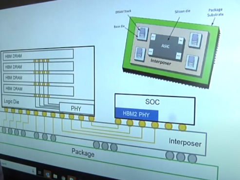
Moreover, says Ferro, HBM2 or HBM2E memories can be linked together in HPC systems.
“How one daisy chains everything together, how the data is moved to the CPU, that is the secret sauce for companies architecting their respective systems,” he states. “Perhaps they have a CPU with its own HBM, or multiple CPUs feeding off a single HBM. These are all potential system designs.”
Commenting on the future beyond HBM2E, Ferro notes that the need for more bandwidth and higher memory densities is only increasing.
“HBM2E uses wide I/O and TSV technologies to support densities up to 24 GB per device at speeds up to 307 GB/s. This bandwidth is delivered across a 1024-bit wide device interface, which is divided into 8 independent channels on each DRAM stack,” he explains. “HBM2E can support 2-high, 4-high, 8-high, and 12-high TSV stacks of DRAM at full bandwidth to allow systems flexibility on capacity requirements from 1 GB – 24 GB per stack.”
As well, says Ferro, HBM2E extends the per pin bandwidth to 3.2 Gbps, adds a new footprint option to accommodate the 16 Gb-layer and 12-high configurations for higher density components, and updates the MISR polynomial options for these new configurations.
Nevertheless, Ferro emphasizes that AI/ML data sets continue to increase at almost exponential rates.
“Even with the improvements offered by HBM2E, system designers are having difficulty keeping up with the massive data sets for AI/ML training. HBM3 is anticipated to deliver much higher bandwidth and densities.”
Commenting on SoC size and chiplets, Ferro points out that costs associated with increasing SoC size has become a significant consideration for the industry.
“We have to look at ways to reduce those costs. We have seen a certain level of disaggregation which has given rise to chiplet technology. There are many reasons aside from a silicon reticle perspective to leverage chiplets,” he elaborates. “One example could be high speed IP that was designed in an earlier node. By using chiplets, a company can take advantage of all that work that was previously developed.”
More specifically, a CPU can be fabbed in the most advanced node, with I/Os in an older node.
“You can also have chips that are I/O bound and then you don’t want to waste silicon. There are a lot of different applications for chiplets going forward. However, system designers will have to determine how a chiplet communicates with the SoC,” he says. “If you are talking to a DRAM – and you have the same HBM PHY – you will have with a monolithic design. But then, as you go back to the CPU, there are different SerDes technologies that are being explored: high speed, very high-speed, and short reach.”
Ferro concludes by noting that high bandwidth memory presents a number of design challenges, as it combines 2.5D and 3D technologies.
“There are a lot of advantages associated with HBM: low power, low area and high bandwidth. However, you must deal with fitting these 2.5D structures in a small area. In addition, maintaining signal integrity is a challenge with traces running at high speeds, as is thermal dissipation from the heat generated by the SoC and the memory itself. Last, but certainly not least, the HBM interposer is a fairly large piece of silicon that presents warping concerns. Nevertheless, even with these design challenges, the performance benefits of HBM are well worth the extra design effort,” he adds.
Leave a Reply