In part 5 of this series, we discussed the most common memory systems that are used in the highest performance AI applications. These include on-chip memory, high bandwidth memory (HBM) and Graphics DDR SDRAM (GDDR SDRAM). In this blog post, we’ll take an in-depth look at on-chip memory, as well as explore some of the primary differences between HBM and GDDR6.
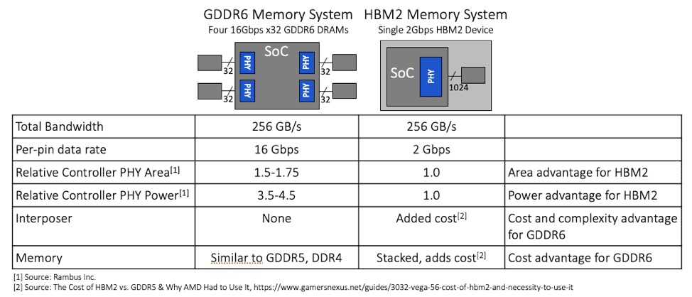
Suppose we set out to design a memory system that provides 256GB/s of memory bandwidth. The slide above illustrates the key differences when implementing such a memory system using HBM2 and GDDR6 DRAMs. As the table illustrates, data rates are one of the primary differences between the two memory types. Because there are fewer data wires, GDDR6 must transmit data at a higher data at a much higher data rate – 16 gigabits per second – as opposed to HBM2 which is running at two gigabits per second with many more wires. As such, the primary challenge associated with GDDR6 is signal integrity, although GDDR6 can enable a lower cost solution because it doesn’t involve intricate stacking like HBM2 does.
Now, let’s take a closer look at the PHY circuits which reside on the SoC and which connect the DRAMs to the SoC. With GDDR6, the amount of area that designers need to reserve on the SoC is between 1.5 and 1.75 times the area required for similar PHY circuits designed to communicate with HBM2 at the same total bandwidth of 256GB/s. In terms of power, it’s a more significant difference, as the GDDR6 PHYs consume anywhere between three-and-a-half to four-and-a-half times as much power as the PHY for an HBM2 implementation at the same bandwidth. From an engineering perspective, there is a definite SoC PHY area and power advantage for HBM2 memory systems.
But the area and power advantages of HBM2 PHYs comes at the expense of higher complexity and cost. This is because HBM2 requires an additional interposer, substrate and intricate stacking within the DRAM as well as between components in the system, all of which add extra cost and complexity, and which are currently exacerbated by the relative newness of the technology. Fundamentally, the decision to use HBM2 or GDDR6 comes down to how you trade off the most important design requirements against what matters most in your system. If you can handle the cost and complexity of an HBM2 implementation, then it is a very good solution. However, if your system requires either more standard manufacturing techniques, or can’t quite absorb the additional costs, then GDDR is a great solution.
On-chip Memory Benefits and Challenges
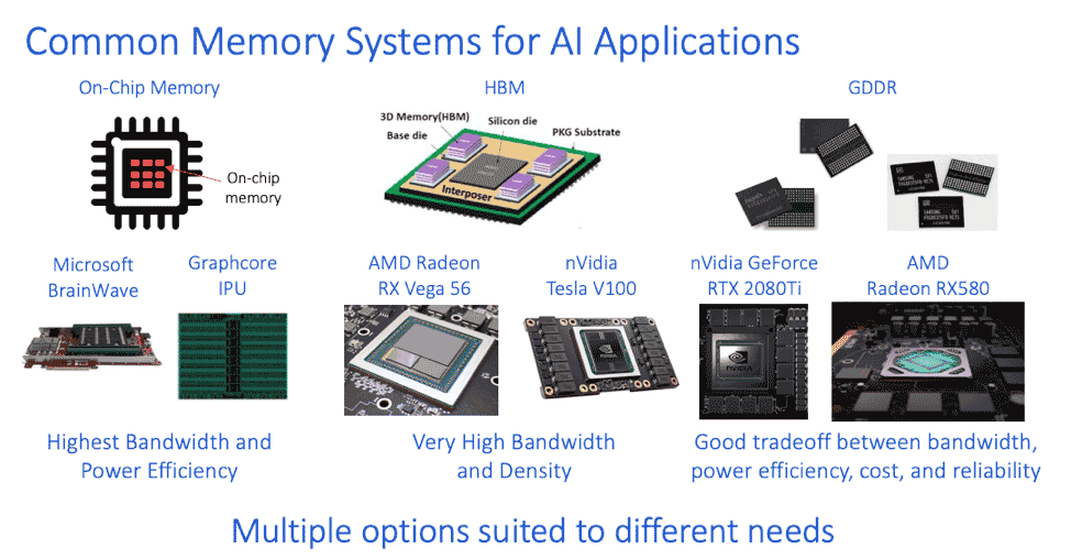
In the latter part of this blog post, we’ll be taking a closer look at the individual types of memories used in AI systems that I referenced earlier so we can walk through the benefits and challenges of each. On the slide above, we can see some of the benefits and challenges of on-chip memory. On-chip memory is used today in solutions such as Microsoft’s Brainwave, Graphcore’s IPU, and Cerebras’ Wafer-Scale Engine. As we’ve previously noted, one of the biggest benefits of on-chip memory is the extremely high bandwidth that it offers.
Today, on-chip memories can deliver on the order of tens of terabytes a second in the largest chips that are about the size of a reticle. On-chip memory also offers extremely low latency and very high-power efficiency, because the data doesn’t need to move very far. The low latency and high bandwidth enable high utilization of the compute engines, even when processing jobs with small batch sizes, which can be particularly important for cloud-based infrastructures.
In terms of challenges and disadvantages, on-chip memory has lower storage capacity compared to external DRAM, although systems designers are implementing some interesting techniques to extend the capacity. For example, instead of saving intermediate results during more complex calculations, results are simply recalculated because it’s cheaper and faster to perform computation than to store and retrieve data from on-chip and external memory. In addition to limited capacity, on-chip memory is challenged by scalability, especially when it comes to large AI models.
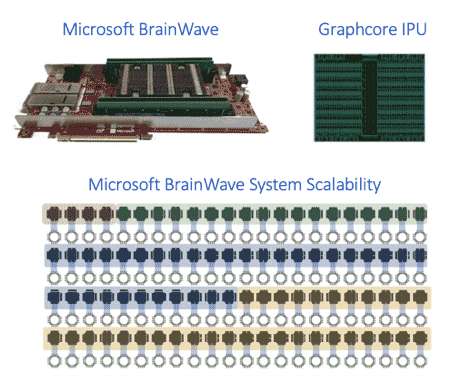
Multiple FPGAs at datacenter scale can form a persistent DNN HW microservice, enabling scale out of models at ultra-low latencies
| Benefits | Challenges |
|---|---|
|
|
On the bottom left of the slide above, the Brainwave approach to system scalability is illustrated by the chaining together of multiple FPGA cards to solve and implement some of their larger networks.
HBM Benefits and Challenges
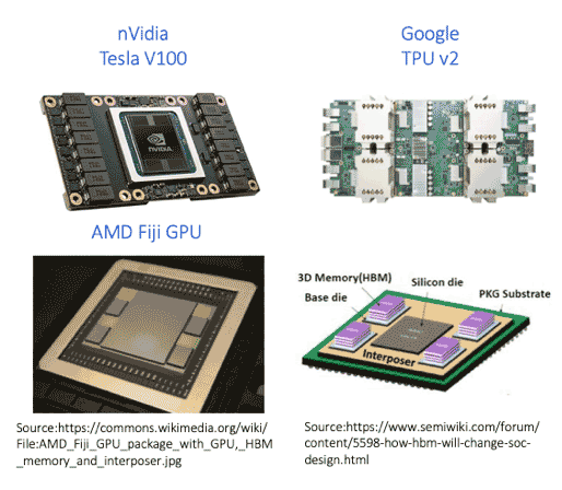
Let’s take a closer look at HBM now. One of the primary benefits of HBM is that it achieves very high bandwidth, the highest bandwidth for any external memory device today, up to 256 gigabytes a second of bandwidth per HBM2 DRAM stack. HBM also offers very good power efficiency because it’s running many I/Os – 1,024 – at a relatively low data rate of two gigabits per second. There are a number of solutions, especially in the AI space, that are adopting HBM2, including nVidia’s Tesla V100 and the second-generation Google TPU.
HBM implementations are challenged by the high number of I/Os which requires a silicon interposer to place the large number of data wires in close proximity to each other. There’s additional cost and design complexity with all the stacking involved, both within the HBM DRAM stack, as well as stacking the components together on top of the interposer and the substrate before it goes onto the PCB. The system engineering challenges associated with this stacking, and the complexity with keeping the silicon cool to maintain reliability, all add to the difficulty of implementing HBM2 solutions. Still, if it’s something that you can tolerate in terms of the cost and the design complexity, HBM2 can be a great choice for external bandwidth solutions.
| Benefits | Challenges |
|---|---|
|
|
GDDR6 Benefits and Challenges
GDDR offers a good middle ground between performance, complexity and cost. So, you can get very high bandwidth and capacity because it is an external type of DRAM that’s already packaged. It’s also easier to integrate, while the system engineering is much simpler compared to a memory type like HBM. GDDR is a great solution for systems that are particularly cost-sensitive or when HBM can’t be easily implemented.
The primary challenge associated with GDDR is running at very high data rates. Although signal integrity becomes more difficult, GDDR is implementable at these speeds with well-designed and well-managed PHYs, packages and boards.
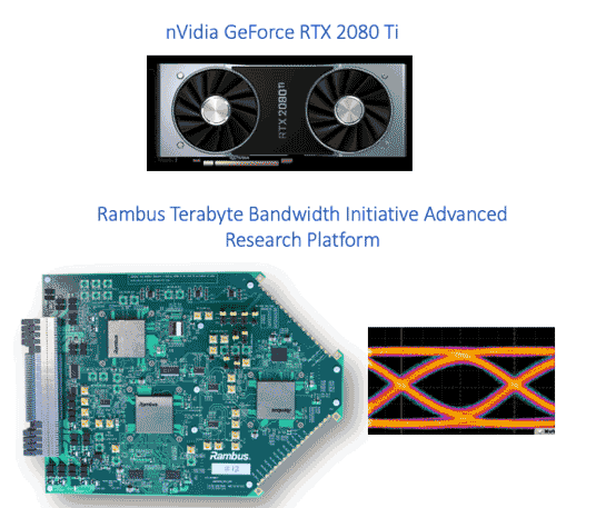
| Benefits | Challenges |
|---|---|
|
|
On the lower left of the slide above, you can see a screen capture and an eye diagram that illustrates some of the work Rambus did several years ago in preparation for achieving GDDR6 data rates. This work proved the ability to signal at these high data rates across standard PCBs and included technology development to enable SoC PHYs to achieve these speeds.
Additional resources:
White Paper: HBM2E and GDDR6: Memory Solutions for AI
Webinar: Memory Systems for AI and Leading-Edge Applications
Webinar: GDDR6 and HBM2E: Memory Solutions for AI
Read more of this series:
Memory Systems for AI: Part 1
Memory Systems for AI: Part 2
Memory Systems for AI: Part 3
Memory Systems for AI: Part 4
Memory Systems for AI: Part 5

Leave a Reply