PCI Express® 4.0 also known as PCIe 4.0 or PCIe Gen 4 is the fourth generation of Peripheral Component Interconnect Express (PCI express) expansion bus specifications, which are developed, published, and maintained by the PCI Special Interest Group (PCI-SIG). It is an open standard.
In this blog, you’ll learn all about PCI express 4 performance vs PCIe 3.0. More specifically:
1. PCIe 4.0 bandwidth
2. Market applications: Who needs PCIe 4.0?
3. PCIe 3.0 vs 4.0: Comparison table
4. PCI Express 4.0 controller IP solutions from Rambus
5. Conclusion
Read our primer? Jump to: PCI Express 5 vs. 4: What’s New?
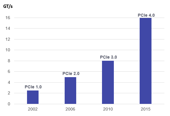
PCIe 4.0 bandwidth
The interconnect performance bandwidth is double that of the PCIe 3.0 specification achieving 16 GT/s and compatibility with software and mechanical interfaces is preserved. PCIe 4.0 architecture is compatible with prior generations of PCIe technology.
Market applications: Who needs PCIe 4.0?
Big Data needs throughput
According to Gary King, Weatherhead University Professor, “The data flow is so fast that the total accumulation of the past two years—a zettabyte—dwarfs the prior record of human civilization”. Internet, ubiquitous smartphone usage and increased marketing accelerated the Big Data revolution, and the Internet of Things (IoT) will increase the needs for fast and efficient data management environments. More throughput and lower power are necessary to prevent a bottleneck in the emergence of Big Data.
Networking applications
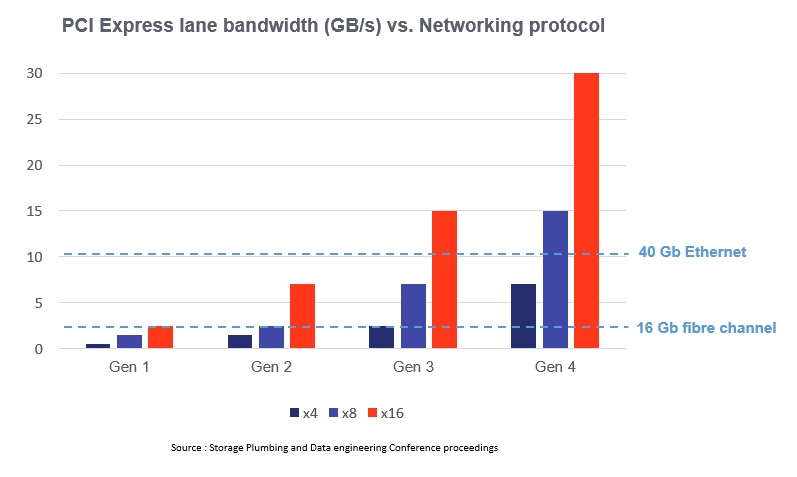
PCIe 4.0 can handle 40Gb Ethernet with an 8-lane configuration, and can handle 100Gb Ethernet (requiring 25 GB/s) with a x16.
PCIe 3.0 vs 4.0: Comparison table
PCIe 4.0 specifications
There are no encoding changes from PCIe 3.0 to 4.0. There were only minor updates in terms of the protocol. There were only minor updates in terms of the protocol.
There were also minor changes in terms of link-level management. PCIe 4.0 enables a more robust equalization.
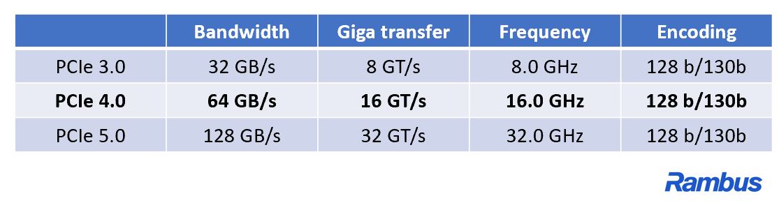
In terms of performance, with PCIe 4.0, throughput per lane is 16 GT/s. The link is full duplex, which means the data can be sent and received simultaneously for a throughput of 32 GT/s per lane. For a x16 configuration, this provides 64 GB/s of bandwidth (16 GT/s x2 (duplex) x16 lanes / 8 bits/byte = 64 GB/s). There is some encoding overhead, the 128b/130b encoding is 98.46% efficient, so actual bandwidth is 63 GB/s.
PCI Express 4.0 controller IP solutions from Rambus
Rambus offers a broad portfolio of PCI Express controller IP from PCIe 2.0 to PCIe 6.0. For PCIe 4.0 specifically, the Rambus PCIe 4.0 Controller IP offers a highly flexible, silicon-proven solution. It can be seamlessly integrated with the customer’s choice of PHY IP.
Why choose Rambus PCIe 4.0 controller IP ?
For the reliability:
- Rambus has over 20 years of experience in the design of IP cores for SoCs with specialization in high-speed interface protocols and technologies with a specific focus on PCIe. This history includes hundreds of successful production tapeouts.
- The proven Rambus PCIe 3.0 architecture is preserved to enable easy migration to PCIe 4.0. No interface change is necessary; existing behavior is preserved for seamless integration
For the flexibility:
Flexibility of the supported PIPE Configurations for PCIe 4.0:
Flexibility of the core configuration to meet spec evolutions
For the supported features:
Features already proven in 3.0, optimized for PCIe 4.0
- Endpoint, root port, switch, dual-mode shared silicon
- Virtualization-ready with SRIOV and ATS/ARI (networking, data center)
- Multi-function
- AER and data integrity mechanism
- Complete power management support: legacy, ASPM L0s/L1, OBFF, L1 PM substate with CLKREQ
- End-end TLP prefixes
- Supports Extension Device ECN
Conclusion
The 4th generation of the PCI Express standard builds on the widely adopted PCIe 3.0 architecture while doubling the link transfer rate to 16 GT/s. In a x16 configuration, PCIe 4.0 supports 100Gb Ethernet and can deliver nearly 64 GB/s of duplex bandwidth. For PCIe 4.0 interface implementations, Rambus offers the silicon-proven PCIe 4.0 Controller IP backed by industry-renowned Rambus service and support.
Keep on reading:
Leave a Reply