Semiconductor Engineering’s Ann Steffora Mutschler recently penned an article about high bandwidth memory (HBM). As Mutschler observes, the latest iteration of HBM continues its rise as a viable contender in the memory space.
Indeed, HBM is finding its way into leading-edge graphics, networking and high-performance computing systems. High bandwidth memory may also find a role in deep learning, artificial intelligence, convolutional neural networking, fully autonomous vehicles, as well as additional advanced applications that demand massive bandwidth and low power.

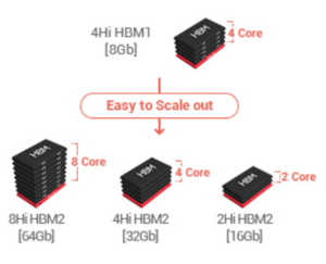
Image Credit: SK Hynix (via Semiconductor Engineering)
“HBM enables lower power consumption per I/O and higher bandwidth memory access with a more condensed form factor, which is enabled by the stacking memory dies directly on top of each other and sharing the same package as an SoC or GPU core using a silicon interposer,” she explained. “Each pin drives a much shorter trace, and runs at a lower frequency, which in turn results in significantly lower switching power.”
High bandwidth performance gains, says Mutschler, are achieved by a very wide I/O parallel interface.
“HBM1 can deliver 128GB/s, while HBM2 offers 256GB/s maximum bandwidth. Memory capacity is easily scaled by adding more dies to the stack, or adding more stacks to the system-in-package,” she elaborated.
According to Frank Ferro, a senior director of product management at Rambus, HBM moves memory closer to the processor using a fatter data pipe, which effectively speeds up data throughput, reduces the amount of power necessary to drive a signal, and cuts RC delay.
“Originally, high-bandwidth memory was seen by the graphics companies as a clear step in the evolutionary direction,” Ferro told the publication. “But then the networking and data center community realized HBM could add a new tier of memory in their memory hierarchy for more bandwidth, and all the things that are driving the datacenter: lower latency access, faster access, less delay, lower power. As a result, HBM design activities have picked up pace in these market segments.”
As noted above, HBM modules are connected to the SoC via a silicon or organic interposer. A short and controlled channel between the memory and the SoC requires less drive from the memory interface, thus reducing the power when compared to DIMM interfaces. In addition, since the interface is wide, system designers can achieve very high bandwidth with a slower frequency.
Perhaps not surprisingly, says Ferro, there are multiple challenges associated with the design of robust HBM2 PHYs.
“One such challenge is maintaining signal integrity at speeds of two gigabits per pin throughout via the interposer. This is why extensive modeling of both signal and power integrity is essential to achieving reliable operation in the field,” he explained in a recent in Semiconductor Engineering article. “As such, HBM PHY design engineers should possess extensive knowledge of 2.5D design techniques, along with a comprehensive understanding of system behavior under various conditions including temperature and voltage variations.”
Determining signal routing tradeoffs via the interposer also presents engineers with another significant challenge. These tradeoffs, says Ferro, entail balancing the ability to maintain optimal system performance while keeping the cost of the interposer as low as possible. For example, design teams must decide if one or two signal routing layers should be used throughout the interposer.
“Although one routing layer saves cost, it demands a more challenging design with narrower channel widths and higher crosstalk,” he continued. “Moreover, design teams need to determine how far apart the ASIC can be moved from the HBM DRAM modules on the interposer. While farther distances can help with thermal dissipation, each millimeter increases the likelihood of signal integrity issues.”
The implementation of 2.5D technology in HBM2 systems adds numerous manufacturing complexities, requiring PHY vendors to work closely with multiple entities, such as semiconductor, manufacturing partner (foundry) and packaging house. As Ferro emphasizes, careful design of the entire system – including SoC, interposer, DRAM and package – are essential to ensure high yield and proper system operation. In addition, having a high yielding module is a critical element of keeping costs in check, given the number of expensive components, including the SoC, multiple HBM die stacks and interposer.
“Even with these challenges, the advantages of having increased memory bandwidth and density closer to the CPU clearly improves overall system efficiency for server and networking systems,” Ferro added.

Leave a Reply