Home > Interface IP > Memory PHYs > LPDDR3 PHY
Memory + Interfaces
LPDDR3 PHY
Fully compliant with LPDDR2 and LPDDR3, our LPDDR3 PHY is part of a complete memory solution designed to meet the demands of the latest generation of mobile devices. When combined with LPDDR3 DRAM, the LPDDR3 memory solution reduces memory system power by up to 25% and supports data rates up to 2133 Mbps, translating to better device performance and improved battery life.
How LPDDR3 PHY works
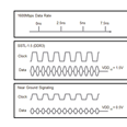
Consumers continue to demand better performance and longer battery life from their mobile devices. Compatible with LPDDR2, LPDDR3 and enhanced LPDDR3, our LPDDR3 PHY delivers on power and performance by supporting data rates up to 2133 Mbps and reducing active memory system power by 25% and active DRAM power by 30%. This reduction in power is made possible through the use of Low Voltage Swing Terminated Logic (LVSTL), a single-ended, ground-terminated signaling technology. LVSTL features a significantly reduced signal swing versus the 1.2 volt High-Speed Unterminated Logic (HSUL) signal swing used in standard LPDDR3. With a reduced signal swing, devices are able to achieve higher data rates with significantly reduced IO power, and subsequently, overall system power.
By supporting both LVSTL and current HSUL signaling, LPDDR3 offers a low-power mode at reduced risk by maintaining compatibility with LPDDR2 and LPDDR3 DRAM standards.
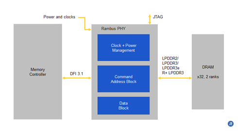
LPDDR3 PHY Subsystem Example
Solution Offerings
- Fully-characterized hard macro (GDSII):
- Complete design views:
- Gate-level and IO models
- Verification test benches
- Layout abstracts (.lef)
- Timing models (.lib)
- Memory controller reference design
- Full Documentation
- Integration Guidelines
- Package and PCB design guidelines
- ASIC/DFT manufacturing guidelines
- Test and Characterization user guide
- Verilog models
- CDL netlists *(.cdl)
- ATPG models
- GDSII layout
- DRC & LVS reports
Memory Suppliers/Manufacturers
- Complete specification and implementation package
- Reference design database including schematics and matching layout
- Integration guidelines
- Package and PCB design guidelines
- Logic and power simulations
- Timing verification environment
- Device characterization and test environment
- Optional design integration and bring-up support services
SOC/ASIC Developers
- Contact LPDDR3 memory supplier for datasheet, roadmap, schedule, and pricing
Comprehensive Chip and System Design Reviews
- Kickoff/Program Review
- Floor plan Review
- Test/Characterization Plan Review
- Package Design Review
- Board Design Review
- Final Chip Integration Review
- Bring-up and Test Review
Engineering Design Services:
- Package design
- System board layout
- Statistically-based signal and power integrity analysis
Protocol Compatibility
| Protocol | Data Rate (Gbps) |
|---|---|
| Rambus LPDDR3 | 200-2133 |
| LPDDR3e | 200-2133 |
| LPDDR3 | 200-1600 |
| LPDDR2 | 200-1066 |
Inventions
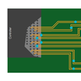
FlexPhase™ Timing Adjustment Circuits
FlexPhase per bit timing adjustment circuits deskew data and clock signals to improve signal integrity and simplify package and PCB system design.
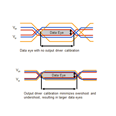
Output Driver Calibration
Output driver calibration allows SoC designers to tune the output signaling to optimal levels in order to improve data rates and system voltage margin.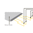
On Die Termination Calibration
ODT calibration enables higher data rates and superior DRAM device and module performance by establishing the optimal termination value to compensate for variations in process and operating conditions that degrade signal performance.
