A new report published by Transparency Market Research confirms the global smart sensor market will hit $21.60 billon by 2019. “Rapidly increasing sales of various
Smart sensor market to hit $21.60 billion by 2019
Double Bus Rate Technology
In many computing systems today, memory bandwidth is a key factor in determining overall system performance, and its importance continues to grow as these systems evolve. Rambus developed a technique for improving memory system bandwidth by increasing the per-pin signaling rate of the data pins of the DRAM. Double Data Rate (DDR) SDRAMs are an example of memory devices that double the per-pin data signaling rate by transferring data on both edges during each clock cycle instead of only on one edge. While such an increase in signaling rate can improve memory bandwidth of the data pins, actual system performance may not improve due to insufficient address/control bandwidth that can reduce data transfer efficiency. To address this problem, Rambus developed Double Bus Rate Technology, an innovation that increases both address/control, and data bandwidth, allowing memory systems to achieve higher levels of performance.
- Increases transfer rate without increase system clock rates
- Improves memory system bandwidth
What is Double Bus Rate Technology?
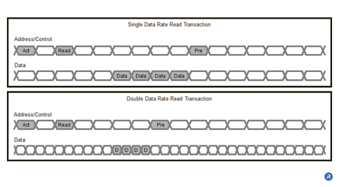
In a read transaction for a single data rate DRAM, the address, control, and data is transferred on one edge of each clock cycle. Memory bandwidth can be improved by applying double bus rate technology and increasing the per-pin data signaling rate of a DRAM. Double Bus Rate Technology allows data to be transferred more quickly, increasing the bandwidth that a DRAM can supply.
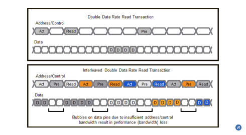
Doubling the data rate of the data transfers affects the relationship between address/control information and data for a Read transaction. When transactions are interleaved, a problem can occur when the amount of time that data occupies the memory bus is smaller than the amount of time that address and control information occupy the bus. In this situation, the insufficient address/control bandwidth leads to bubbles in the data transfer on the bus, resulting in reduced memory bandwidth and loss of performance.
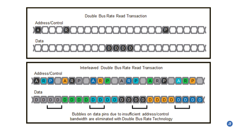
The issue of performance loss can be addressed by applying Double Bus Rate Technology to the address and control pins as well. Double Bus Rate Technology is used to balance address, control, and data bandwidth, thereby eliminating the concerns relating to insufficient address and control bandwidth. As a result, bandwidth is increased by 50% compared to the interleaved transactions with double bus rate technology. Another example of where increased control bandwidth can be useful is in systems that use write masking. In systems that utilize write masking, increasing the amount of data being transferred to memory requires that more byte masking control information be specified in order to maintain support for data masking at byte granularities. By balancing address, control, and data transfer rates on the bus with Double Bus Rate Technology, performance losses due to insufficient address and control bandwidth are eliminated.
Who Benefits?
Many groups can benefit from double bus rate technology. By balancing address, control, and data bandwidth, system designers are able to achieve the highest levels of memory bandwidth in their systems. This in turn helps to reduce the number of DRAMs necessary to achieve a given level of memory performance, reducing component count and easing system component placement, routing concerns, and thermal dissipation. System designers and integrators benefit from the reduced component count needed to achieve a given level of memory bandwidth, resulting in lower system cost and smaller form-factor systems.
Asymmetric Equalization
[fullwidth background_color=”” background_image=”” background_parallax=”none” enable_mobile=”no” parallax_speed=”0.3″ background_repeat=”no-repeat” background_position=”left top” video_url=”” video_aspect_ratio=”16:9″ video_webm=”” video_mp4=”” video_ogv=”” video_preview_image=”” overlay_color=”” overlay_opacity=”0.5″ video_mute=”yes” video_loop=”yes” fade=”no” border_size=”0px” border_color=”” border_style=”” padding_top=”20″ padding_bottom=”20″ padding_left=”0″ padding_right=”0″ hundred_percent=”no” equal_height_columns=”no” hide_on_mobile=”no” menu_anchor=”” class=”” id=””][one_full last=”yes” spacing=”yes” center_content=”no” hide_on_mobile=”no” background_color=”” background_image=”” background_repeat=”no-repeat” background_position=”left top” border_position=”all” border_size=”0px” border_color=”” border_style=”” padding=”” margin_top=”” margin_bottom=”” animation_type=”” animation_direction=”” animation_speed=”0.1″ class=”” id=””][fusion_text]Enables very high bandwidth on next generation memory systems. Signal equalization is applied asymmetrically across the memory PHY and DRAM communication link and improves overall signal integrity while minimizing the complexity and cost of the DRAM device. [Read more…] about Asymmetric Equalization
Securing ultra-low-power devices
Ernest Worthman of Semiconductor Engineering recently noted that future ultra-low-power (ULP) IoT devices require a new paradigm for handling cryptography. “To optimize the power in
VirtuOptic™ Reflectors
VirtuOptic™ reflectors deliver a highly efficient, collimated light pattern that can be evenly distributed over wide areas, making it ideal for high brightness architectural, entertainment and commercial lighting applications. When combined with Rambus’ proprietary optical modeling and design techniques, the shape and size of the VirtuOptic reflectors can be optimized to achieve a highly-controlled, directed light output at the desired ray angle for minimal glare.
- Greater than 90% optical efficiency
- Reduced glare with a highly-controlled, collimated light output
- Even light distribution over wide areas
What is VirtuOptic Reflector Technology?
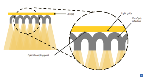
VirtuOptic™ Reflectors take advantage of the optical property of total internal reflection (TIR), which is an extremely efficient means of transporting light. Light is injected into the end of a light guide using Rambus’ TruEdge™ LED coupling technology. It is transmitted down the length of the light guide through TIR with minimal loss, producing a uniform emission of light from the reflective optical elements.
VirtuOptic™ Reflectors are created by bonding an array of high precision reflectors to an optical light guide, using a material with a matching refractive index. Light is extracted from the light guide at the optical coupling points at the center of each VirtuOptic™ Reflector in a near zero-loss transition, creating a uniform array of virtual light sources.
Who Benefits?
Light fixture designers can take advantage of the high-efficiency and unique aesthetic of the virtual light sources created by VirtuOptic™ Reflectors to create cost-effective fixtures with customizable light outputs. The even light distribution produced enables commercial lighting specifiers to save costs and reduce the total number of fixtures required to deliver the desired amount of light to a given surface.
Very Low-Swing Differential Signaling
Today’s mobile device demand high bandwidth for HD video capture and streaming, and media-rich web browsing as well as extended battery life. Very Low-Swing Differential Signaling (VLSD) is a bi-directional, ground-referenced, differential signaling technology which offers a high-performance, low-power, and cost-effective solution for applications requiring extraordinary bandwidth and superior power efficiency.
- Enables high data rates at very low IO power consumption
- Improves signal integrity
What is Very Low-Swing Differential Signaling Technology?
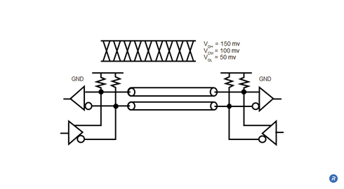
VLSD signals are point-to-point and use an ultra-low 100mV signal swing (50 to 150mV) and 100mV common-mode voltage, which results in a 200mV peak-to-peak differential signal swing. This swing is less than 1/10th the signaling swing of commodity memory interfaces. VLSD enables high data rates with very low IO power consumption.
Who Benefits?
VLSD enables system designers to achieve high-speed operation through the robust signaling characteristics inherent to differential signaling, while minimizing IO power consumption through the use of a ground-referenced low-voltage-swing signaling system. This combination of high-bandwidth and low-power operation improves mobile device performance and battery life for consumers.