The PLDA PCIe Controller for USB4 with AXI supports the PCIe 5.0 specification, and implements the required features mandated by the USB4 Specification. The controller can be configured to support endpoint, root port, switch port, and dual-mode topologies, allowing for a variety of use models.
PCIe Controller for USB4 Product Brief
The PLDA PCIe Controller for USB4 supports the PCIe 5.0 specification, and implements the required features mandated by the USB4 Specification. The controller can be configured to support endpoint, root port, switch port, and dual-mode topologies, allowing for a variety of use models.
PCIe Switch for USB4 Product Brief
The PLDA PCIe Switch for USB4 is a customizable, embedded switch for PCI Express (PCIe) designed for implementations in USB4 devices.
Rambus Completes Acquisition of PLDA
Extends CXL™ and PCI Express® Digital IP Leadership
SAN JOSE, Calif. – August 18, 2021 – Rambus Inc. (NASDAQ: RMBS), a provider of industry-leading chips and silicon IP making data faster and safer, today announced the completion of the acquisition of PLDA. With this acquisition, Rambus expands its digital controller offerings with complementary CXL 2.0, PCIe 5.0 and PCIe 6.0 controller and switch IP, and gains critical building blocks for its CXL Memory Interconnect Initiative.
“CXL and PCIe are critical enablers for next-generation data centers that will deliver the high-speed interconnects needed to tackle demanding workloads in AI/ML and HPC applications,” said Luc Seraphin, president and CEO of Rambus. “The addition of PLDA’s world-class digital IP and engineering expertise accelerates our roadmap and expands our market opportunity, and we are excited to welcome them to the team.”
Although this transaction will not materially impact 2021 financial results due to the timing of close and acquisition accounting, Rambus expects this acquisition to be accretive in 2022.
For more information, visit rambus.com/plda.
Forward-looking statements
Information set forth in this press release, including statements as to Rambus’ outlook and statements as to the expected timing, completion and effects of the acquisition, constitute forward-looking statements within the meaning of the safe harbor provisions of the Private Securities Litigation Reform Act of 1995.
These statements are based on various assumptions and the current expectations of the management of Rambus and may not be accurate because of risks and uncertainties surrounding these assumptions and expectations. Factors listed below, as well as other factors, may cause actual results to differ significantly from these forward-looking statements. There is no guarantee that any of the events anticipated by these forward-looking statements will occur, or what effect they will have on the operations or financial condition of Rambus. Forward-looking statements included herein are made as of the date hereof, and Rambus undertakes no obligation to publicly update or revise any forward-looking statement unless required to do so by federal securities laws.
Major risks, uncertainties and assumptions include, but are not limited to: the expected benefits and costs of the proposed transaction; management’s plans relating to the proposed transaction; the expected timing and completion of the proposed transaction; statements of the plans, strategies and objectives of Rambus for future operations; any statements regarding anticipated operational and financial results; any statements of expectation or belief; the risk that disruptions from the proposed transaction will harm Rambus’ business; other factors described under “Risk Factors” in Rambus’ Annual Report on Form 10-K and Quarterly Reports on Form 10-Q; and any statements of assumptions underlying any of the foregoing. It is not possible to predict or identify all such factors. Consequently, while the list of factors presented here is considered representative, no such list should be considered to be a complete statement of all potential risks and uncertainties.
CCIX 1.1 Controller with AXI Product Brief
The PLDA CCIX 1.1 Controller with AXI supports the PCI Express 5.0, 4.0 and 3.1/3.0 specifications, as well as with version 4.x and 5.x of the PHY Interface for PCI Express (PIPE) specification, and supports the CCIX Extended Speed Mode as defined in the CCIX Base Specification Revision 1.1.
Rambus Advances AI/ML Performance with 8.4 Gbps HBM3-Ready Memory Subsystem
Highlights:
- Provides HBM3-ready memory subsystem solution consisting of fully-integrated PHY and digital controller
- Supports data rates up to 8.4 Gigabits per second (Gbps), enabling terabyte-scale bandwidth accelerators for artificial intelligence/machine learning (AI/ML) and high-performance computing (HPC) applications
- Leverages market-leading HBM2/2E experience and installed-base to speed implementation of customer designs using next-generation HBM3 memory
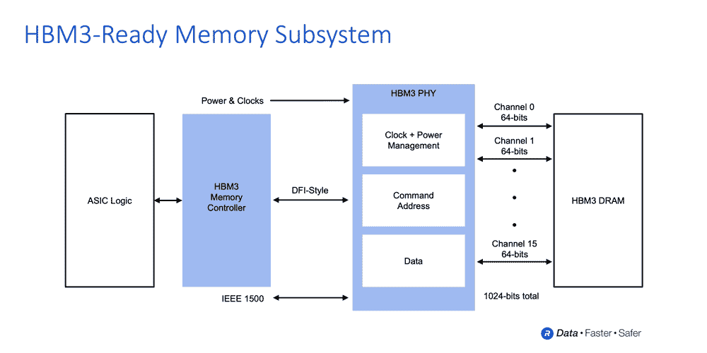
SAN JOSE, Calif. – Aug. 16, 2021 – Rambus Inc. (NASDAQ: RMBS), a premier chip and silicon IP provider making data faster and safer, today announced the Rambus HBM3-ready memory interface subsystem consisting of a fully-integrated PHY and digital controller. Supporting breakthrough data rates of up to 8.4 Gbps, the solution can deliver over a terabyte per second of bandwidth, more than double that of high-end HBM2E memory subsystems. With a market-leading position in HBM2/2E memory interface deployments, Rambus is ideally suited to enable customers’ implementations of accelerators using next-generation HBM3 memory.
“The memory bandwidth requirements of AI/ML training are insatiable with leading-edge training models now surpassing billions of parameters,” said Soo Kyoum Kim, associate vice president, Memory Semiconductors at IDC. “The Rambus HBM3-ready memory subsystem raises the bar for performance enabling state-of-the-art AI/ML and HPC applications.”
Rambus achieves HBM3 operation of up to 8.4 Gbps leveraging over 30 years of high-speed signaling expertise, and a strong history of 2.5D memory system architecture design and enablement. In addition to the fully-integrated HBM3-ready memory subsystem, Rambus provides its customers with interposer and package reference designs to speed their products to market.
“With the performance achieved by our HBM3-ready memory subsystem, designers can deliver the bandwidth needed by the most demanding designs,” said Matt Jones, general manager of Interface IP at Rambus. “Our fully-integrated PHY and digital controller solution builds on our broad installed base of HBM2 customer deployments and is backed by a full suite of support services to ensure first-time right implementations for mission-critical AI/ML designs.”
Benefits of the Rambus HBM3-ready Memory Interface Subsystem:
- Supports up to 8.4 Gbps data rate delivering bandwidth of 1.075 Terabytes per second (TB/s)
- Reduces ASIC design complexity and speeds time to market with fully-integrated PHY and digital controller
- Delivers full bandwidth performance across all data traffic scenarios
- Supports HBM3 RAS features
- Includes built-in hardware-level performance activity monitor
- Provides access to Rambus system and SI/PI experts helping ASIC designers to ensure maximum signal and power integrity for devices and systems
- Includes 2.5D package and interposer reference design as part of IP license
- Features LabStation™ development environment that enables quick system bring-up, characterization and debug
- Enables the highest performance in applications including state-of-the-art AI/ML training and high-performance computing (HPC) systems
For more information on the Rambus Interface IP, including our PHYs and Controllers, please visit rambus.com/interface-ip.