Signal integrity (SI) is a perennial issue with system and SoC designers. As design engineers begin to launch into next generation systems with GDDR6 DRAMs, they’ll encounter new rounds of signal integrity issues not faced before. Rambus experts are currently taking a hard look at the issue to come up with answers to this difficult problem that involves a host of associated contributors to signal integrity.
The Signal Integrity Journal defines it as: “Signal integrity covers all the issues about single ended and differential signal propagation from the transmitter to the receiver, including problems such as impedance control, discontinuities, reflections, topology, terminations, losses, ISI, jitter, eye diagrams, cross talk and ground bounce.”
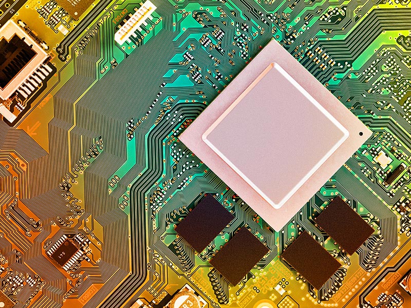
Having said that, with GDDR6, signal integrity goes well beyond the chip and core levels as most savvy SI experts know. Today, GDDR6 DRAM vendors and their technical research staffs are placing major emphasis investigating not only chip and core signal integrity problematic areas, but also going into the printed circuit board (PCB) design.
PCB design questions arising deal with the correct surface finishes and whether to use blind or buried vias and if so, what effects are there on SI and the design tradeoffs that have to be made. Plus, there are a multitude of questions dealing with PCB design when it comes to SI.
But, for starters, Rambus SI experts say there are three main SI losses. Those are insertion loss, reflections, and crosstalk.
Insertion loss is due to dielectric loss or metal surface roughness. The more surface roughness, the more there is a DC-like loss. At high frequency, that loss increases, and from the dielectric side, dielectric loss tangents cause attenuation on the signal. However, the receiver can control this type of loss. Usually, there are amplifiers, gains, and filters like continuous time linear equalization (CTLE), which can correct this loss.
Reflections occur when the signal goes through the fabric. It transitions from the chip to the package, onto the PCB) and then on to the DRAM package. Through these transitions, the signal goes from a bump to the trace on the package, and then through the vias, and then through the ball-grid array (BGA) package and on to the PCB.
Also, it’s inevitable that the signal goes over a void. A void is found in a BGA ball solder joint to the BGA interface, or in the solder joint to the PCB interface. It causes an impedance discontinuity, which in turn causes the signal to reflect. These reflections cause the eye to eye closure and loss of signaling.
But citing these three losses is but the tip of the iceberg when it comes to GDDR6 DRAM signal integrity issues designers will be confronted with. There’s more. So, stay tuned.
Leave a Reply