LED Fixture Light Guides Solution Overview
Beginning with edge-lit back lighting, Rambus has pioneered light guide-based design solutions for a broad range of LED lighting applications, enabling a new level of styling, efficiency and control of light.
We combined TruEdge™ LED Coupling – techniques to maximize the amount of light emitted from the LED to the light guide – with MicroLens® optics – micro 3D features that provide controlled light extraction – to create highly-efficient and cost-effective solutions with unparalleled design flexibility.
Our offering includes customizable light guide design and manufacturing solutions with expert optical engineering support. The light guides are available as off-the-shelf or customized designs that are optimized to specific customer and application requirements by varying the size, shape and density of the MicroLens optics. These light guides can be manufactured by our global lighting partners or at our state-of-the-art facility within the US.
Complete fixture prototype designs that combine Rambus optical innovations with design engineering and manufacturing support services are also available to lighting system companies and fixture manufacturers worldwide.
Lensless Smart Sensors Solution Overview
Imaging and smart sensors are essential for the Internet of Things to become a reality. In order for the objects and machines around us to adapt and anticipate our changing needs, they must be able to gather and act upon relevant data from their surroundings quickly and cost-effectively.
We have pioneered a new class of computational imagers ideally suited for ubiquitous sensing with our ultra-miniature Lensless Smart Sensors (LSS). LSS take a novel approach to reduce the size, cost and power consumption for sensing and imaging by replacing the lens with a low-cost diffraction grating attached directly to the image sensor array. Each grating has a unique design that creates a predictable and pattern on the sensor that is used to capture data-rich images and information about its surroundings.
The gratings and sensors are combined with computational algorithms optimized for specific applications. The net result is a smart sensor with a smaller form factor, better power efficiency, greater precision, and lower cost compared to a traditional image sensor with computer vision. LSS can be used for a broad range of tasks including point tracking, gesture recognition, change detection, motion flow and range finding.
Test Vector Leakage Assessment (TVLA) Derived Test Requirements (DTR) with AES
This document describes requirements and test procedures for qualifying DPA-resistant implementations of cryptographic algorithms with specific instructions and test vectors for AES. Expected lab and analyst proficiency, device setup, data acquisition, signal processing, analysis and evaluation procedures are described herein.
Download “Test Vector Leakage Assessment (TVLA) Derived Test Requirements (DTR) with AES”
Binary Pixel Imagers Solution Overview
Our Binary Pixel technology combines a breakthrough imager and processing architecture to enable professional quality images from mobile phones and point-and-shoot consumer cameras. The technology mimics the brilliance of human visual processing by sensing photons using discrete thresholds similar to the rods and cones of the human eye.
This “binary operation” allows the imager to capture the full gamut of details in dark and bright by using discrete thresholds to avoid pixel saturation and enable better light sensitivity. Binary Pixel also uses spatial oversampling which sub-divides Individual pixels to capture more data and extend dynamic range of the imager.
In addition, innovative processing improves low-light capture and enhances stop-motion performance for dramatically sharper images of moving objects. The net result is significantly improved image quality and performance in a form factor ideal for mobile devices.
Near Ground Signaling
Reduced power consumption has become of key importance in memory system design—from mobile to enterprise-class applications. In addition to clocking power and DRAM core access power, IO signaling power must be addressed in order to reduce the total power consumption of the memory system. Near ground signaling is a single-ended, ground-terminated technology theat enables high data rates at greatly reduced IO signaling power while reducing design complexity by supporting significantly reduced signal swings of 500 millivolts (mV) and below.
- Supports high-speed operation with reduced IO signaling power
- Improved signal integrity
- Reduced design complexity
- Eliminates the need for thick-oxide transistors on memory controller
- Reduced voltage is better matched to advanced processes
What is Near Ground Signaling Technology?
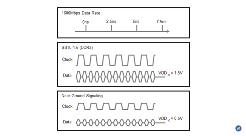
Near Ground Signaling (NGS) is a single-ended, ground-terminated signaling technology that enables high data rates at significantly reduced Input Output (IO) signaling power and design complexity, while maintaining excellent signal integrity. With a VDDIO of 0.5V, Near Ground Signaling has a reduced signal swing compared to traditional Stub Series Terminated Logic (SSTL) signaling and lowers IO power on both the DRAM and controller.
This lower IO voltage is better matched to the operating voltage of advanced CPU’s and GPU’s and reduces the cost and complexity of integrating the memory controller on the processor chip.
Who Benefits?
Memory designers benefit from the reduced design complexity, lowering their integrated memory controller implementation costs. They are also able to achieve increased data rates at significantly reduces IO signaling power.
Commercial server managers and consumer end users benefit from the reduced cost of ownership and increased battery life for their end systems and devices.