Our CryptoManager Provisioning automates and secures the provisioning of device services across the supply chain, reducing operating costs and accelerating time-to-market. It is designed to easily integrate into any manufacturing facility without disruption to existing operations.
On-Chip Noise Monitor Product Brief
Our On-Chip Power Supply Noise Monitor has been developed to overcome the characterization challenges of low-power, high-performance interfaces and electronic systems. It is a compact IP block embedded on-chip and works in conjunction with our LabStation™ Validation Platform to enable noise measurements directly on the chip.
LabStation Validation Platform Product Brief
Design complexity for advanced SoCs rises with each new process node, performance increase, and addition of new IP blocks. Designers are faced with increasing challenges to confidently verify and validate functionality of their chips. The LabStation Validation platform is a comprehensive tool suite for the rapid bring-up, validation and characterization of complex low-power, high-performance memory and serial link IP. It is designed to be easy to use and improve productivity while providing improved accuracy of test results and confidence is system performance.
LPDDR3 DRAM Product Brief
LPDDR3 PHY Product Brief
Fully compliant with LPDDR3 and LPDDR2 DRAM specifications, our LPDDR3 PHY pairs with the LPDDR3 DRAM to create a memory subsystem that supports data rates of up to 2133 Mbps, and reduces active memory system power by up to 25% and active DRAM power by up to 30%. This enables a significantly improved thermal profile and an increased battery life in the end device. The improved thermal profile also enables the memory system to run at peak bandwidth for longer periods of time, which translates to better overall performance in the end systems.
The improvement in power consumption is a result of Low Voltage Swing Terminated Logic (LVSTL), a single-ended, ground-terminated signaling technology, used while in R+ mode. LVSTL features a significantly reduced signal swing versus the 1.2 volt HSUL (High Speed Unterminated Logic) signal swing of standard LPDDR3. Reduced signal swing translates to significantly reduced IO power at high data rate, which is a major component of DRAM power. By supporting LVSTL and HSUL signaling, LPDDR3 offers a low-power mode while maintaining compatibility with LPDDR3 and LPDDR2 DRAM standards.
Phase Interpolator-Based CDR
In order to communicate data from one chip to another across a signal line, the receiving chip must know when to sample the data signal that it receives from the transmitting chip. In many systems, this information is provided by a timing (clock) signal sent from the transmitting chip to the receiving chip along a dedicated timing signal line adjacent to the data signal line. In systems with higher signaling rates, the receiving chip typically requires a clock alignment circuit, such as a Phase Locked Loop (PLL) or Delay Locked Loop (DLL), but the data timing must still be well-matched in order to eliminate timing skews. A phase interpolator based clock-data recovery circuit (CDR) is an alternative circuit architecture developed by Rambus which provides multiple advantages compared to PLL-based CDRs.
- Reduces cost, power and area of a CDR
- Improves jitter performance in high-speed links
What is Phase Interpolator-Based CDR Technology?
Buffered modules introduce a memory buffer between the memory controller and the DRAM devices on each module, isolating the DRAM from the memory bus and enabling an increase to the width of the memory without increasing the pin count of the controller. This also reduces the effective capacitive load on the memory bus enabling support for multiple modules at high speed.
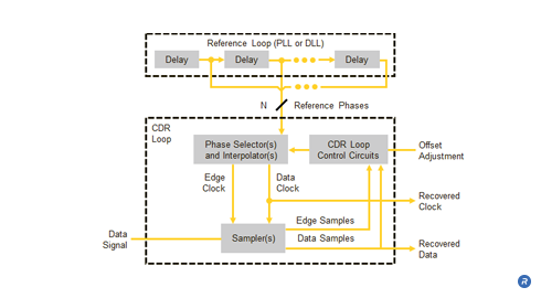
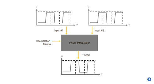
A phase-interpolator based CDR is an alternative circuit architecture developed by Rambus which provides multiple advantages compared to PLL-based CDRs. This type of CDR uses a PLL or DLL to implement a reference loop which accepts an input reference clock signal and produces a set of high speed clock signals, used as reference phases, spaced evenly across 360 degrees. These reference phases are then fed to a CDR loop which includes circuitry for selecting pairs of reference phases and interpolating between them to provide clocks for recovering the data from the data signal.
Because of the separation between the reference loop and the CDR loop, the designer of a phase interpolator based CDR can separately optimize both the noise suppression of the reference loop and the tracking agility of the CDR loop. Additionally, the reference loop is not affected by the contents of the data signal, potentially allowing this type of CDR to track a wider variety of data signals. Furthermore, the relatively long locking time of the reference loop applies only at start-up when initially locking to the reference clock signal. After the initial locking time, interpolator-based CDRs can provide much faster re-locking compared to PLL-based CDRs whenever the data signal returns after being interrupted.
Another benefit of phase interpolator based CDRs is that the data sampling point can be precisely adjusted by a digitally controlled offset. This allows the cancellation of offsets from device mismatches and other causes, and enables in-system measurements of the timing margin available for reliably extracting data from the data signal.
Lastly, although the reference loop can occupy the majority of the area and dissipate the majority of the power in a phase interpolator based CDR, its reference phases can be shared among several CDR loops on chips receiving multiple data signals. In this way, the average size and power required for the CDR functionality per data signal can be greatly reduced.
Who Benefits?
The use of phase interpolator based CDRs benefits many different groups. By designing ASICs including Rambus IO cells that utilize phase interpolator based CDRs, ASIC vendors benefit from the smaller area, lower power, and more stable operation of the IO cells. These benefits are magnified when dual, quad, or other multi-lane IO cells are used since these cells use one reference loop to drive multiple CDR loops for implementing multiple CDRs. The area and power savings can be significant compared to using a PLL per lane, as required by other CDR designs. The ability to digitally offset the data sampling clock when using a phase interpolator based CDR allows in-system testing of timing margins in the actual operating environment. Such system-level testing increases the reliability of manufactured systems for system integrators. Finally, the cost, power, performance, and testability benefits from using phase interpolator based CDRs is passed along to products purchased by consumers in the form of lower prices, longer battery life, and improved reliability.