The design of chip anti-tamper protection needs to adapt and scale with rising threats. Adversaries range from high school hackers to well-funded state actors. Given the threats, it’s useful to think about anti-tamper countermeasures as a hierarchy of safeguards that parallel the type, effort and expense of attacks.
Rambus Demonstrates HBM2E Running at 4 Gbps: 512 GB/s per HBM2E Stack
Rambus has demonstrated that its HBM2E solution, which consists of a memory controller and a verified 1024-bit PHY, can operate at a whopping 4.0 Gbps data transfer rate per pin. The demonstration is meant to prove potential clients that the HBM2E solution can scale and offer a 25% higher peak bandwidth than is officially defined by JEDEC’s HBM2E standard.
Rambus Advances HBM2E Performance to 4.0 Gbps for AI/ML Training Applications
Highlights:
- Fully-integrated HBM2E memory interface solution, consisting of verified PHY and controller, achieves industry’s fastest performance
- New benchmark in performance supports accelerators requiring terabyte-scale bandwidth for artificial intelligence/machine learning (AI/ML) training applications
- Partners with SK hynix and Alchip to develop 2.5D HBM2E memory system solution using TSMC N7 process and CoWoS® advanced packaging technologies
- Offers unrivaled system expertise supporting customers with interposer and package reference designs to speed time to market
Read first our primer on:
HBM2E Implementation & Selection – The Ultimate Guide »
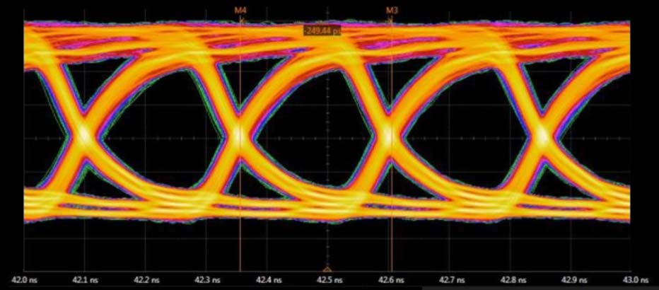
SAN JOSE, Calif. – Sept. 9, 2020 – Rambus Inc. (NASDAQ: RMBS), a premier silicon IP and chip provider making data faster and safer, today announced it has achieved a record 4 Gbps performance with the Rambus HBM2E memory interface solution consisting of a fully-integrated PHY and controller. Paired with the industry’s fastest HBM2E DRAM from SK hynix operating at 3.6 Gbps, the solution can deliver 460 GB/s of bandwidth from a single HBM2E device. This performance meets the terabyte-scale bandwidth needs of accelerators targeting the most demanding AI/ML training and high-performance computing (HPC) applications.
“With this achievement by Rambus, designers of AI and HPC systems can now implement systems using the world’s fastest HBM2E DRAM running at 3.6 Gbps from SK hynix,” said Uksong Kang, vice president of product planning at SK hynix. “In July, we announced full-scale mass-production of HBM2E for state-of-the-art computing applications demanding the highest bandwidth available.”
The fully-integrated, production-ready Rambus HBM2E memory subsystem runs at 4 Gbps without PHY voltage overdrive. Rambus teamed with SK hynix and Alchip to implement the HBM2E 2.5D system to validate in silicon the Rambus HBM2E PHY and Memory Controller IP using TSMC’s N7 process and CoWoS® (Chip-on-Wafer-on-Substrate) advanced packaging technologies. Co-designing with the engineering team from Rambus, Alchip led the interposer and package substrate design.
“This advancement of Rambus and its partners, using TSMC’s advanced process and packaging technologies, is another important achievement of our ongoing collaboration with Rambus,” said Suk Lee, senior director of the Design Infrastructure Management Division at TSMC. “We look forward to a continued partnership with Rambus to enable the highest performance in AI/ML and HPC applications.”
“Alchip brought a demonstrated track record of success in 7nm and 2.5D package design to this initiative,” said Johnny Shen, CEO of Alchip Technologies. “We’re extremely proud of our contributions to Rambus’ breakthrough achievement.”
Rambus has 30 years of high-speed memory design applied to the most demanding computing applications. Its renowned signal integrity expertise was key to achieving an HBM2E memory interface capable of 4 Gbps operation. This raises a new benchmark for meeting the insatiable bandwidth requirements of AI/ML training.
“With silicon operation up to 4 Gbps, designers can future-proof their HBM2E implementations and can be confident of ample margin for 3.6 Gbps designs,” said Matthew Jones, senior director and general manager of IP cores at Rambus. “As part of every customer engagement, Rambus provides reference designs for the 2.5D package and interposer to ensure first-time right implementations for mission-critical AI/ML designs.”
Benefits of the Rambus HBM2E Memory Interface (PHY and Controller):
- Achieves the industry’s highest speed of 4 Gbps per pin, delivering a system bandwidth of 460 GB from a single 3.6 Gbps HBM2E DRAM 3D device.
- Fully-integrated and verified HBM2E PHY and Controller reduces ASIC design complexity and speeds time to market
- Includes 2.5D package and interposer reference design as part of IP license
- Provides access to Rambus system and SI/PI experts helping ASIC designers to ensure maximum signal and power integrity for devices and systems
- Features LabStation™ development environment that enables quick system bring-up, characterization and debug
- Supports high-performance applications including state-of-the-art AI/ML training and high-performance computing (HPC) systems
For more information on the Rambus Interface IP, including our PHYs and Controllers, please visit rambus.com/interface-ip.
Micron Reveals GDDR6X Details: The Future of Memory, or a Proprietary DRAM?
Micron Technology shared some additional details about its latest GDDR6X SGRAM used by Nvidia’s GeForce RTX 30-series graphics cards at a virtual briefing last week. The company revealed that it has experimented for more than a decade with technologies enabling the new type of memory and said that GDDR6X SGRAM had not been standardized by JEDEC yet. Right now, only Nvidia uses GDDR6X memory, but Micron hopes this will change over time. Can it?
Rambus and Micron Extend Patent License Agreement
SAN JOSE, Calif. – Sept 3, 2020 – Rambus Inc. (Nasdaq: RMBS), a premier silicon IP and chip provider making data faster and safer, today announced it has extended its patent license agreement with Micron for an additional four years. The extension maintains the existing financial terms of the agreement and provides Micron with a license to the extensive portfolio of Rambus patents until December 1, 2024.
“We are very pleased Micron has extended their patent license agreement and with how our broader relationship has grown over time,” said Kit Rodgers, senior vice president of technology partnerships and corporate development at Rambus. “We look forward to our continued collaboration in the future.”
Micron Spills on GDDR6X: PAM4 Signaling For Higher Rates, Coming to NVIDIA’s RTX 3090
It would seem that Micron this morning has accidentally spilled the beans on the future of graphics card memory technologies – and outed one of NVIDIA’s next-generation RTX video cards in the process. In a technical brief that was posted to their website, dubbed “The Demand for Ultra-Bandwidth Solutions”, Micron detailed their portfolio of high-bandwidth memory technologies and the market needs for them. Included in this brief was information on the previously-unannounced GDDR6X memory technology, as well as some information on what seems to be the first card to use it, NVIDIA’s GeForce RTX 3090.