[Last updated on: July 29, 2024] On July 14th, 2021, JEDEC announced the publication of the JESD79-5 DDR5 SDRAM standard signaling the industry transition to DDR5 server and client dual-inline memory modules (DIMMs). DDR5 memory brings a number of key performance gains to the table, as well as new design challenges. Computing system architects, designers, and purchasers want to know what’s new in DDR5 vs DDR4 and how they can get the most from this new generation of memory.
In this article:
Performance: what changes in DDR5 vs DDR4 DRAM?
The top seven most significant specification advances made in the transition from DDR4 to DDR5 DIMMs are shown in the table below.
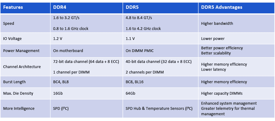
DDR5 changes and advantages over DDR4 DIMMs
1. DDR5 Scales to 8.4 GT/s
You can never have enough memory bandwidth, and DDR5 helps feed that insatiable need for speed. While DDR4 DIMMs top out at 3.2 gigatransfers per second (GT/s) at a clock rate of 1.6 gigahertz (GHz), initial DDR5 DIMMs delivered a 50% bandwidth increase to 4.8 GT/s. DDR5 memory will ultimately scale to a data rate of 8.4 GT/s. New features, such as Decision Feedback Equalization (DFE), were incorporated in DDR5 enabling the higher IO speeds and data rates.
2. Lower Voltage Keeps Power Manageable
A second major change is a reduction in operating voltage (VDD), and that helps offset the power increase that comes with running at higher speed. With DDR5, the DRAM, the registering clock driver (RCD) voltage drops from 1.2 V down to 1.1 V. Command/Address (CA) signaling is changed from SSTL to PODL, which has the advantage of burning no static power when the pins are parked in the high state.
3. New Power Architecture for DDR5 DIMMs
A third change, and a major one, is power architecture. With DDR5 DIMMs, power management moves from the motherboard to the DIMM itself. DDR5 DIMMs will have a 12-V power management IC (PMIC) on DIMM allowing for better granularity of system power loading. The PMIC distributes the 1.1 V VDD supply, helping with signal integrity and noise with better on-DIMM control of the power supply.
4. DDR5 vs DDR4 Channel Architecture
Another major change with DDR5, number four on our list, is a new DIMM channel architecture. DDR4 DIMMs have a 72-bit bus, comprised of 64 data bits plus eight ECC bits. With DDR5, each DIMM will have two channels. Each of these channels will be 40-bits wide: 32 data bits with eight ECC bits. While the data width is the same (64-bits total) having two smaller independent channels improves memory access efficiency. So not only do you get the benefit of the speed bump with DDR5, the benefit of that higher MT/s is amplified by greater efficiency.
In the DDR5 DIMM architecture, the left and right side of the DIMM, each served by an independent 40-bit wide channel, share the RCD. In DDR4, the RCD provides two output clocks per side. In DDR5, the RCD provides four output clocks per side. In the highest density DIMMs with x4 DRAMs, this allows each group of 5 DRAMs (single rank, half-channel) to receive its own independent clock. Giving each rank and half-channel an independent clock improves signal integrity, helping to address the lower noise margin issue raised by lowering the VDD (from change #2 above).
5. Longer Burst Length
The fifth major change is burst length. DDR4 burst chop length is four and burst length is eight. For DDR5, burst chop and burst length will be extended to eight and sixteen to increase burst payload. Burst length of sixteen (BL16), allows a single burst to access 64 Bytes of data, which is the typical CPU cache line size. It can do this using only one of the two independent channels. This provides a significant improvement in concurrency and with two channels, greater memory efficiency.
6. DDR5 Supports Higher Capacity DRAM
A sixth change to highlight is DDR5’s support for higher capacity DRAM devices. With DDR5 buffer chip DIMMs, the server or system designer can use densities of up to 64 Gb DRAMs in a single-die package. DDR4 maxes out at 16 Gb DRAM in a single-die package (SDP). DDR5 supports features like on-die ECC, error transparency mode, post-package repair, and read and write CRC modes to support higher-capacity DRAMs. The impact of higher capacity devices obviously translates to higher capacity DIMMs. So, while DDR4 DIMMs can have capacities of up to 64 GB (using SDP), DDR5 SDP-based DIMMs quadruple that to 256 GB.
7. A Smarter DIMM with DDR5
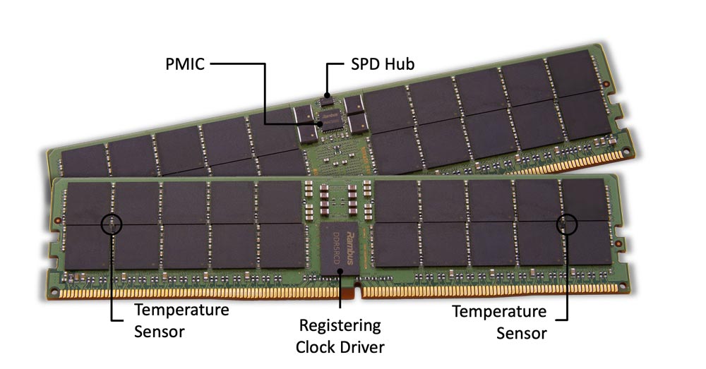
The DDR5 server DIMM chipset replaces the DDR4 SPD IC with an SPD Hub IC and adds two temperature sensor (TS) ICs. The SPD Hub has an integrated TS, which in conjunction with the two discrete TS ICs, provides three points of thermal telemetry from the RDIMM.
With DDR5, the communication bus between chips gets an upgrade to I3C running 10X faster than the I2C bus used in DDR4. The DDR5 SPD Hub handles communication from the module to the Baseboard Management Controller (BMC). Using the faster I3C protocol, the DDR5 SPD Hub reduces initialization time and supports a higher rate of polling and real-time control.
Thermal information, communicated from the SPD Hub to the BMC, can be used to manage cooling fan speed. DRAM refresh rate can now be more finely managed to provide for higher performance or higher retention, and if the RDIMM is running too hot, bandwidth can be throttled as needed to reduce the thermal load.
What are the DDR5 Design Challenges?
These changes in DDR5 introduce a number of design considerations dealing with higher speeds and lower voltages – raising a new round of signal integrity challenges. Designers will need to ensure that motherboards and DIMMs can handle the higher signal speeds. When performing system-level simulations, signal integrity at all DRAM locations needs to be checked.
For DDR4 designs, the primary signal integrity challenges were on the dual-data-rate DQ bus, with less attention paid to the lower-speed command address (CA) bus. For DDR5 designs, even the CA bus will require special attention for signal integrity. In DDR4, there was consideration for using differential feedback equalization (DFE) to improve the DQ data channel. But for DDR5, the RCD’s CA bus receivers will also require DFE options to ensure good signal reception.
The power delivery network (PDN) on the motherboard is another consideration, including up to the DIMM with the PMIC. Considering the higher clock and data rates, you will want to make sure that the PDN can handle the load of running at higher speed, with good signal integrity, and with good clean power supplies to the DIMMs.
The DIMM connectors from the motherboard to the DIMM will also have to handle the new clock and data rates. For the system designer, at the higher clock speeds and data rates around the printed circuit board (PCB), more emphasis must be placed on system design for electromagnetic interference and compatibility (EMI and EMC).
How do DDR5 memory interface chipsets harness the advantages of DDR5 for DIMMs?
The good news is that DDR5 memory interface chips improve signal integrity for the command and address signals sent from the host memory controller to the DIMMs. The bus for each of the two channels goes to the RCD and then fans out to the two halves of the DIMM. The RCD effectively reduces the loading on the CA bus that the host memory controller sees.
The expanded chipset including PMIC, SPD Hub and TS enable a smarter DIMM which can operate at the higher data rates of DDR5 while remaining within the desired power and thermal envelope.
Rambus offers a full DDR5 memory interface chipset that helps designers harness the full advantages of DDR5 while dealing with the signal integrity challenges of higher data, CA and clock speeds. Rambus was the first in the industry to deliver a DDR5 RCD to 5600 MT/s and is continually advancing the performance of its DDR5 solutions to meet growing market needs. The Rambus DDR5 RCD has now reached performance levels of 7200 MT/s.
As DDR5 evolves and makes its way to the client space, the Rambus DDR5 client memory interface chipset enables client DIMMs (CSODIMMs and CUDIMMs) to deliver new levels of memory performance for demanding gaming, content creation and AI workloads on PCs. The DDR5 Client DIMM Chipset includes a DDR5 Client Clock Driver (CKD) and Serial Presence Detect Hubs (SPD Hub).
As a renowned leader in signal integrity (SI) and power integrity (PI), Rambus has over 30 years’ experience in enabling the highest performance systems in the market.
Additional resources on DRR5:
– What’s Next for DDR5 Memory?
– Data Center Evolution: DDR5 DIMMs Advance Server Performance
Leave a Reply