Steven Woo, Rambus fellow and distinguished inventor, recently spoke with Ed Sperling of Semiconductor Engineering about designing systems with GDDR6 and HBM2. As Woo emphasizes, understanding engineering tradeoffs are an important part of deciding how to best match a system with the most appropriate memory.
Read first our primer on:
HBM2E Implementation & Selection – The Ultimate Guide »
“HBM2 is newer and requires a broader range of engineering skills to implement. If you can design with it, HBM2 can provide a number of advantages,” says Woo. “GDDR6 relies on more established types of older design experience that many people have. However, while HBM is typically used for the highest performance tasks, engineers are adapting whichever memory is the best for their application. It really is about a set of design trade-offs.”
Standard PCB Versus an Interposer
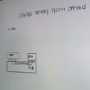
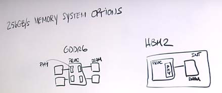
In the images below and video above, Woo uses a standard 256 gigabyte per second memory system to highlight some of the design tradeoffs of GDDR6 and HBM2.
“To implement a 256 gigabyte per second system with GDDR6, we will connect four DRAMs to the GPU. There is also a standard PCB – and you simply connect the GPU to the DRAM through standard connections that go right into the PCB,” he explains.

“This is a very common connection topology and very simple – something that is very commonly done in the industry. So, it relies on a lot of historical experience.”
Implementing the system in HBM2 says Woo, is an altogether different experience.
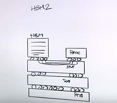
“The DRAMs are newer technology – a stack of DRAM die all packaged together. The DRAM die stack is connected to the processor,” he elaborates.

“Now, what’s really interesting about this is that instead of having a small number of connections like you do with GDDR6, HBM2 requires a much larger number of connections. We’re talking on the order of a thousand, for which you can’t use a standard PCB because it’s not designed to have that many connections.”
Instead, says Woo, HBM2 uses a silicon interposer to accommodate very small and fine pitch wires.
“You can put many of them together. This allows you to take the many I/Os that you need to connect your HBM device stack to your processor and do it all in one interposer,” he explains. “However, you eventually have to get that interposer or assembly on to a standard PCB. So, what you need in between is the substrate, which acts a bit like a gasket. It allows you to take that silicon interposer assembly and put it directly onto a PCB.”
As Woo notes, there are more complicated structures and layers that need to be properly implemented before an HBM2-based memory system is completely and correctly assembled.
“HBM2 does take more skill to design with. It’s a newer technology that requires additional steps and cost,” he states. “Nevertheless, HBM2 is currently being used in advanced systems across a range of verticals. For example, you see it used in AI and very high-end graphics systems.”
Signal Integrity, Die Stacks and Limited I/O
In terms of signal integrity, says Woo, HBM2 has considerably more interconnects than its GDDR6 counterpart, although the former runs at slower speeds.
“It is easier to maintain signal integrity from that standpoint – but the trade-off is the complexity in building this type of system and making it reliable,” he adds. “You have more components that you have to put together under different kinds of stresses as the system operates. This means HBM2 system level reliability can be very different than what you would see in a more traditional GDDR6 system.”
Regarding HBM2 die stacks, Woo observes that there is a complex interplay between stack capacity and other variables to consider.
“You’re going to eventually want to put more devices into the stack and you’re going to have to balance that with how many I/Os you can actually run through an interposer. So, there are various complex design trade-off questions to answer,” he explains. “For example, how expensive do you want the interposer to be and how will that influence the number of wires you have? Also, how many devices do you want in the stack? And what does the bandwidth need to be to adequately feed the processor with all that data?”
Bandwidth & PHYs
With regard to bandwidth and PHYs, Woo notes that there are critical circuits on the system processor known as the PHY which connect the processor to the DRAM.
“There’s a big difference between the PHY area and power that you need to dedicate on that processor when it comes to the two memory types,” he says.

“The question is how much area on that processor silicon you need to dedicate to real estate in order to talk to those DRAMs. What we’ve found is that GDDR6 takes anywhere between one and a half to one point seven five times more area than it does for HBM2.”
In terms of design trade-offs between GDDR6 and HBM2, Woo points out that the GDDR6 system DRAM has a small number of pins running at a high data rate of 16 gigabits per second. However, the HBM2 system has many more interconnects, in fact, well over a thousand.
“This means you can actually get the same bandwidth by running each of those I/Os at a much lower data rate. In this particular case (the 256 gigabyte per second memory system), it’s just two gigabits per second,” he says.
With regards to PHY power consumption, says Woo, there is actually a big difference between a GDDR6 and HBM2 system. More specifically, GDDR6 consumes three and a half to four and a half times the power on the PHY compared to HBM2.
Interested in learning more about system design with HBM2 and GDDR6? You can check out our HBM2 PHY product page here and our GDDR6 PHY product page here.

Leave a Reply