• Skip to primary navigation
  • Skip to main content
  • Skip to footer
  • English
  • Investor Relations
  • Resource Library
  • Newsroom
  • Blog
  • Careers
  • Support Center
Rambus Logo

Rambus

At Rambus, we create cutting-edge semiconductor and IP products, spanning memory and interfaces to security, smart sensors and lighting.

  • Products
      • All
          • Memory Interface Chips
          • DIMM Chipsets
          • DDR5 DIMM Chipset
          • DDR4 NVRCD
          • DDR4 Register Clock Driver
          • DDR4 Data Buffer
          • CXL Memory Interconnect Initiative
          • Interface IP
          • Memory PHYs
          • GDDR6 PHY
          • HBM3 PHY
          • HBM2E PHY
          • DDR4 PHY
          • More…
          • SerDes PHYs
          • PCIe 5.0 PHY
          • PCIe 4.0 PHY
          • 32G C2C PHY
          • 32G PHY
          • 28G PHY
          • More…
          • Digital Controllers
          • Memory Controllers
          • CXL & PCI Express Controllers
          • MIPI Controllers
          • Video Compression and Forward Error Correction Cores
          • Security IP
          • Root of Trust Solutions
          • Security Protocol Engines
          • Inline Cipher Engines
          • Crypto Accelerator Cores
          • DPA Countermeasures
          • Software Protocols & Crypto Toolkits
          • Anti-Counterfeiting
          • Provisioning and Key Management
      • Memory Interface Chips
        • DIMM Chipsets
          • DDR5 DIMM Chipset
          • Non-Volatile DDR4 Registering Clock Driver
          • DDR4 Register Clock Driver
          • DDR4 Data Buffer
          • DDR3 Register Clock Driver
          • DDR3 Isolation Memory Buffer
        • CXL Memory Interconnect Initiative

        • Made for high speed, reliability and power efficiency, our DDR3, DDR4, and DDR5 DIMM chipsets deliver top-of-the-line performance and capacity for the next wave of computing systems. Learn more about our Memory Interface Chip solutions
      • Interface IP
          • Memory PHYs
            • GDDR6 PHY
            • HBM3 PHY
            • HBM2E PHY
            • DDR4 PHY
            • DDR4 Multi-modal PHY
            • DDR3 PHY
          • SerDes PHYs
            • PCIe 5.0 PHY
            • PCIe 4.0 PHY
            • 32G C2C PHY
            • 32G PHY
            • 28G PHY
            • 16G PHY
            • 12G PHY
            • 6G PHY
          • Digital Controllers
            • HBM3 Controller
            • HBM2E Controller
            • GDDR6 Controller
            • LPDDR5 Controller
            • CXL 2.0 Controller
            • PCIe 6.0 Controller
            • PCIe 5.0 Controller
            • MIPI CSI-2/DSI-2 Controllers
            • Video Compression and Forward Error Correction Cores
            • More…

        • With their reduced power consumption and industry-leading data rates, our line-up of memory interface IP solutions support a broad range of industry standards with improved margin and flexibility. Learn more about our Interface IP solutions
      • Security IP
          • Root of Trust Solutions
          • Security Protocol Engines
            • MACsec Engines
            • IPsec, TLS, SSL Multi-Protocol Engines
            • High Speed Public Key Accelerator
          • Inline Cipher Engines
          • Crypto Accelerator Cores
            • DPA Resistant Cores
            • Basic Crypto Blocks
          • Anti-Counterfeiting
            • CryptoFirewall Cores
            • Circuit Camouflage Technology
          • DPA Countermeasures
            • DPA Resistant Cores
            • DPA Resistant Software Libraries
            • DPA Workstation Platform
          • Software Protocols & Crypto Toolkits
            • IPsec Toolkit
            • FIPs Cryptographic Libraries
            • MACsec Toolkit
            • IoT Security Framework
          • CryptoMedia
            • Content Protection Core
            • Content Protection Services
          • Provisioning and Key Management
            • CryptoManager Provisioning
            • CryptoManager Device Key Management

        • From chip-to-cloud-to-crowd, Rambus secure silicon IP helps protect the world’s most valuable resource: data. Securing electronic systems at their hardware foundation, our embedded security solutions span areas including root of trust, tamper resistance, content protection and trusted provisioning. Learn more about our Security IP offerings
  • Markets
      • AI & Machine Learning
        • Speed and Security for the Artificial Intelligence & Machine Learning Revolution
          • Products
          • SerDes PHYs
          • Memory PHYs
          • Digital Controllers
          • Memory Interface Chips
          • Root of Trust
          • Crypto Accelerator Cores
          • Protocol Engines
          • Provisioning and Key Management
          • AI & Machine Learning
      • Automotive
        • Providing Performance & Security for the Connected Car
          • Products
          • Memory PHYs
          • SerDes PHYs
          • Digital Controllers
          • Root of Trust
          • PKE Engine
          • MACsec Engines
          • Crypto Accelerator Cores
          • Provisioning and Key Management
          • Explore Automotive
      • Data Center
        • Optimizing capacity, connectivity and capability of the cloud
          • Products
          • SerDes PHYs
          • Memory PHYs
          • Digital Controllers
          • Memory Interface Chips
          • Root of Trust
          • MACsec Engines
          • Software Protocols
          • Provisioning and Key Management
          • See Data Center
      • Edge
        • Catching a tidal wave of data
          • Products
          • Memory PHYs
          • SerDes PHYs
          • Digital Controllers
          • Root of Trust
          • Crypto Accelerator Cores
          • Protocol Engines
          • Software Protocols
          • Discover Edge
      • Government
        • Securing Mission-critical Systems
          • Products
          • Root of Trust
          • Protocol Engines
          • Anti-Tamper Cores
          • Provisioning and Key Management
          • DPA Workstation Platform
          • SerDes PHYs
          • Memory PHYs
          • Digital Controllers
          • See Government
      • IoT
        • Making IoT Data Safe & Fast
          • Products
          • Root of Trust
          • TLS Toolkits
          • Provisioning and Key Management
          • Memory PHYs
          • SerDes PHYs
          • Digital Controllers
          • Explore IoT
  • Resources
    • Inventions
    • Buying Guide
    • Resource Library
      • Webinars
      • Product Selector
  • About
      • Corporate Overview
      • Leadership
      • Inventors
      • Careers
      • Locations
      • Investor Relations
      • Newsroom
      • Blog
      • Events
      • Partnerships
      • Corporate Responsibility
      • Contact
Home > Inventions > Page 2

Inventions

DPA Countermeasures

Many electronic devices that use cryptography are susceptible to side channel attacks. These low-cost, non-invasive methods enable attackers to extract the secret cryptographic keys used during normal device operations by monitoring a device’s timing, power consumption, or electromagnetic emissions. Side channel attacks leave no trace, and can often be performed quickly using consumer-level equipment. Once the secret keys have been extracted, attackers can gain unauthorized access, decrypt or forge messages, steal identities, clone devices, create unauthorized signatures, and perform other unauthorized transactions. DPA Countermeasures are fundamental techniques developed to protect against side channel attacks—safeguarding billions of devices from unauthorized use and access.

  • Superior protection against side channel attacks
  • Simplified device testing for power analysis vulnerabilities

What are DPA Countermeasures?

Cryptographic key extraction using differential Power Analysis (DPA)

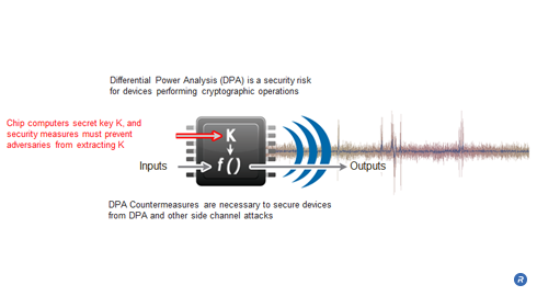
Simple Power Analysis (SPA) and Differential Power Analysis (DPA) are powerful, non-invasive side channel attacks that allow adversaries to compromise the security of tamper-resistant devices by analyzing their power consumption. SPA recovers secret keys through direct observation of a device’s power consumption, while DPA attacks employ statistical techniques to extract secret key information from multiple power consumption measurements. DPA can extract secret keys in a noisy environment where the power consumption of the cryptographic computation is a very small fraction of the overall power consumption of a system. DPA Countermeasures were developed to protect tamper-resistant devices against side channel attacks including SPA, DPA and related electromagnetic (EM) attacks.

DPA Countermeasures consist of a broad range of software, hardware, and protocol techniques that protect tamper-resistant devices from side channel attacks in a number of ways including:

  • Leak reduction – reducing information leaked into the side channel to decrease signal-to-noise (S/N) ratios
  • Amplitude and temporal noise – adding amplitude or temporal noise into the side channel to decrease S/N ratio
  • Balanced hardware and software – using hardware and software-based techniques to represent and process data in ways designed to minimize observable data-dependent variations within the side channel
  • Incorporating randomness – representing cryptographic intermediates in forms that incorporate unpredictable information to reduce correlation between side channels and the original intermediates
  • Protocol-level countermeasures – modifying cryptographic protocols using key update mechanisms to limit the amount of side channel information available to an attacker for any particular key

Who Benefits?

Device and system manufacturers, and end users benefit from the high-levels of security that are provided at the hardware level to protect against side channel attacks. Devices and industries that benefit from DPA Countermeasures include telecommunications, payments and banking, entertainment, pay television, government and defense, mobile devices, automotive, smart cards, media storage and integrated circuits.

Double Bus Rate Technology

In many computing systems today, memory bandwidth is a key factor in determining overall system performance, and its importance continues to grow as these systems evolve. Rambus developed a technique for improving memory system bandwidth by increasing the per-pin signaling rate of the data pins of the DRAM. Double Data Rate (DDR) SDRAMs are an example of memory devices that double the per-pin data signaling rate by transferring data on both edges during each clock cycle instead of only on one edge. While such an increase in signaling rate can improve memory bandwidth of the data pins, actual system performance may not improve due to insufficient address/control bandwidth that can reduce data transfer efficiency. To address this problem, Rambus developed Double Bus Rate Technology, an innovation that increases both address/control, and data bandwidth, allowing memory systems to achieve higher levels of performance.

  • Increases transfer rate without increase system clock rates
  • Improves memory system bandwidth

What is Double Bus Rate Technology?

Single data rate and double data rate read transactions

In a read transaction for a single data rate DRAM, the address, control, and data is transferred on one edge of each clock cycle. Memory bandwidth can be improved by applying double bus rate technology and increasing the per-pin data signaling rate of a DRAM. Double Bus Rate Technology allows data to be transferred more quickly, increasing the bandwidth that a DRAM can supply.

Interleaved double date rate read transactions without Double Bus Rate technology

Doubling the data rate of the data transfers affects the relationship between address/control information and data for a Read transaction. When transactions are interleaved, a problem can occur when the amount of time that data occupies the memory bus is smaller than the amount of time that address and control information occupy the bus. In this situation, the insufficient address/control bandwidth leads to bubbles in the data transfer on the bus, resulting in reduced memory bandwidth and loss of performance.

Interleaved double bus rate read transactions without Double Bus Rate technology

The issue of performance loss can be addressed by applying Double Bus Rate Technology to the address and control pins as well. Double Bus Rate Technology is used to balance address, control, and data bandwidth, thereby eliminating the concerns relating to insufficient address and control bandwidth. As a result, bandwidth is increased by 50% compared to the interleaved transactions with double bus rate technology. Another example of where increased control bandwidth can be useful is in systems that use write masking. In systems that utilize write masking, increasing the amount of data being transferred to memory requires that more byte masking control information be specified in order to maintain support for data masking at byte granularities. By balancing address, control, and data transfer rates on the bus with Double Bus Rate Technology, performance losses due to insufficient address and control bandwidth are eliminated.

Who Benefits?

Many groups can benefit from double bus rate technology. By balancing address, control, and data bandwidth, system designers are able to achieve the highest levels of memory bandwidth in their systems. This in turn helps to reduce the number of DRAMs necessary to achieve a given level of memory performance, reducing component count and easing system component placement, routing concerns, and thermal dissipation. System designers and integrators benefit from the reduced component count needed to achieve a given level of memory bandwidth, resulting in lower system cost and smaller form-factor systems.

Asymmetric Equalization

[fullwidth background_color=”” background_image=”” background_parallax=”none” enable_mobile=”no” parallax_speed=”0.3″ background_repeat=”no-repeat” background_position=”left top” video_url=”” video_aspect_ratio=”16:9″ video_webm=”” video_mp4=”” video_ogv=”” video_preview_image=”” overlay_color=”” overlay_opacity=”0.5″ video_mute=”yes” video_loop=”yes” fade=”no” border_size=”0px” border_color=”” border_style=”” padding_top=”20″ padding_bottom=”20″ padding_left=”0″ padding_right=”0″ hundred_percent=”no” equal_height_columns=”no” hide_on_mobile=”no” menu_anchor=”” class=”” id=””][one_full last=”yes” spacing=”yes” center_content=”no” hide_on_mobile=”no” background_color=”” background_image=”” background_repeat=”no-repeat” background_position=”left top” border_position=”all” border_size=”0px” border_color=”” border_style=”” padding=”” margin_top=”” margin_bottom=”” animation_type=”” animation_direction=”” animation_speed=”0.1″ class=”” id=””][fusion_text]Enables very high bandwidth on next generation memory systems. Signal equalization is applied asymmetrically across the memory PHY and DRAM communication link and improves overall signal integrity while minimizing the complexity and cost of the DRAM device. [Read more…] about Asymmetric Equalization

VirtuOptic™ Reflectors

VirtuOptic™ reflectors deliver a highly efficient, collimated light pattern that can be evenly distributed over wide areas, making it ideal for high brightness architectural, entertainment and commercial lighting applications. When combined with Rambus’ proprietary optical modeling and design techniques, the shape and size of the VirtuOptic reflectors can be optimized to achieve a highly-controlled, directed light output at the desired ray angle for minimal glare.

  • Greater than 90% optical efficiency
  • Reduced glare with a highly-controlled, collimated light output
  • Even light distribution over wide areas

What is VirtuOptic Reflector Technology?

VirtuOptic™ reflector technology

VirtuOptic™ Reflectors take advantage of the optical property of total internal reflection (TIR), which is an extremely efficient means of transporting light. Light is injected into the end of a light guide using Rambus’ TruEdge™ LED coupling technology. It is transmitted down the length of the light guide through TIR with minimal loss, producing a uniform emission of light from the reflective optical elements.

VirtuOptic™ Reflectors are created by bonding an array of high precision reflectors to an optical light guide, using a material with a matching refractive index. Light is extracted from the light guide at the optical coupling points at the center of each VirtuOptic™ Reflector in a near zero-loss transition, creating a uniform array of virtual light sources.

Who Benefits?

Light fixture designers can take advantage of the high-efficiency and unique aesthetic of the virtual light sources created by VirtuOptic™ Reflectors to create cost-effective fixtures with customizable light outputs. The even light distribution produced enables commercial lighting specifiers to save costs and reduce the total number of fixtures required to deliver the desired amount of light to a given surface.

Very Low-Swing Differential Signaling

Today’s mobile device demand high bandwidth for HD video capture and streaming, and media-rich web browsing as well as extended battery life. Very Low-Swing Differential Signaling (VLSD) is a bi-directional, ground-referenced, differential signaling technology which offers a high-performance, low-power, and cost-effective solution for applications requiring extraordinary bandwidth and superior power efficiency.

  • Enables high data rates at very low IO power consumption
  • Improves signal integrity

What is Very Low-Swing Differential Signaling Technology?

Very low-swing differential signaling circuit diagram

VLSD signals are point-to-point and use an ultra-low 100mV signal swing (50 to 150mV) and 100mV common-mode voltage, which results in a 200mV peak-to-peak differential signal swing. This swing is less than 1/10th the signaling swing of commodity memory interfaces. VLSD enables high data rates with very low IO power consumption.

Who Benefits?

VLSD enables system designers to achieve high-speed operation through the robust signaling characteristics inherent to differential signaling, while minimizing IO power consumption through the use of a ground-referenced low-voltage-swing signaling system. This combination of high-bandwidth and low-power operation improves mobile device performance and battery life for consumers.

TruEdge™ LED Coupling

The growing popularity of LEDs in general lighting applications has introduced great opportunities for a new generations of energy-efficient lighting, but LEDs are not without their difficulties. Designers are challenged with how to transform single, or multiple point sources of light into an aesthetically-pleasing, uniform distribution of light. The use of edge-lit architectures—where LEDs are placed along one or more edges of a light guide—is a highly-efficient means of directing and distributing light. A key component to those architectures, TruEdge™ LED coupling technology optimizes the interface between the LED light source and the light guide to maximize the amount of light injected into the light guide. By combining Rambus’ proprietary optical modeling and design techniques, TruEdge technology can achieve 93 to 96% LED-to-light guide coupling efficiency.

  • Optimizes LED-to-light guide interface to maximize coupling efficiency
  • Reduces fixture cost with fewer LEDs
  • Enables thinner form factors

What is TruEdge™ LED Coupling Technology?

TruEdge™ LED coupling technology

TruEdge™ LED Coupling coupling enables highly-efficient, edge-lit general lighting fixtures that utilize the fewest number of LEDs for a desired light output level. Edge-lit systems can be implemented in a myriad of form factors while producing aesthetically pleasing, diffuse light with minimal glare. This is achieved by optimizing the interface between the LED and light guide through the use of reflectors, couplings lenses and tight LED-to-light guide integration. The combination of these techniques maximizes the efficiency of coupling interface and, in turn, the amount of light delivered from the fixture.

Who Benefits?

When implemented in an edge-lit architecture, TruEdge™ LED Coupling coupling delivers tremendous flexibility of form factor and freedom of design without sacrificing efficiency or control. This will enable designers to create a new age of beautiful and functional lighting. End users will also benefit from the energy-efficient and cost-effective fixtures that are made possible with TruEdge technology.

  • « Go to Previous Page
  • Go to page 1
  • Go to page 2
  • Go to page 3
  • Go to page 4
  • Go to page 5
  • Go to Next Page »

Footer

About

  • Corporate Overview
  • Leadership
  • Careers
  • Locations
  • Investor Relations
  • News
  • Corporate Responsibility

Products

  • Memory PHYs
  • SerDes PHYs
  • Digital Controllers
  • Server DIMM Chipsets
  • Root of Trust Solutions
  • Provisioning and Key Management
  • Protocol Engines
  • Crypto Accelerator Cores
  • Software Protocols
  • DPA Countermeasures
  • Anti-Counterfeiting
  • CryptoMedia

Markets

  • AI & Machine Learning
  • Automotive
  • Data Center
  • Edge
  • Government
  • IoT
  • Pay TV

Resources

  • Resource Library
  • Webinars
  • Inventions
  • Buying Guide
  • Contact

Copyright © 2022 Rambus.com. All Rights Reserved. Privacy Policy | Trademark & Guidelines

  • Facebook icon
  • Twitter icon
  • YouTuve icon
  • LinkedIn icon
  • Blog icon