• Skip to primary navigation
  • Skip to main content
  • Skip to footer
  • English
  • Investor Relations
  • Resource Library
  • Newsroom
  • Blog
  • Careers
  • Support Center
Rambus Logo

Rambus

At Rambus, we create cutting-edge semiconductor and IP products, spanning memory and interfaces to security, smart sensors and lighting.

  • Products
      • All
          • Memory Interface Chips
          • DIMM Chipsets
          • DDR5 DIMM Chipset
          • DDR4 NVRCD
          • DDR4 Register Clock Driver
          • DDR4 Data Buffer
          • CXL Memory Interconnect Initiative
          • Interface IP
          • Memory PHYs
          • GDDR6 PHY
          • HBM3 PHY
          • HBM2E PHY
          • DDR4 PHY
          • More…
          • SerDes PHYs
          • PCIe 5.0 PHY
          • PCIe 4.0 PHY
          • 32G C2C PHY
          • 32G PHY
          • 28G PHY
          • More…
          • Digital Controllers
          • Memory Controllers
          • CXL & PCI Express Controllers
          • MIPI Controllers
          • Video Compression and Forward Error Correction Cores
          • Security IP
          • Root of Trust Solutions
          • Security Protocol Engines
          • Inline Cipher Engines
          • Crypto Accelerator Cores
          • DPA Countermeasures
          • Software Protocols & Crypto Toolkits
          • Anti-Counterfeiting
          • Provisioning and Key Management
      • Memory Interface Chips
        • DIMM Chipsets
          • DDR5 DIMM Chipset
          • Non-Volatile DDR4 Registering Clock Driver
          • DDR4 Register Clock Driver
          • DDR4 Data Buffer
          • DDR3 Register Clock Driver
          • DDR3 Isolation Memory Buffer
        • CXL Memory Interconnect Initiative

        • Made for high speed, reliability and power efficiency, our DDR3, DDR4, and DDR5 DIMM chipsets deliver top-of-the-line performance and capacity for the next wave of computing systems. Learn more about our Memory Interface Chip solutions
      • Interface IP
          • Memory PHYs
            • GDDR6 PHY
            • HBM3 PHY
            • HBM2E PHY
            • DDR4 PHY
            • DDR4 Multi-modal PHY
            • DDR3 PHY
          • SerDes PHYs
            • PCIe 5.0 PHY
            • PCIe 4.0 PHY
            • 32G C2C PHY
            • 32G PHY
            • 28G PHY
            • 16G PHY
            • 12G PHY
            • 6G PHY
          • Digital Controllers
            • HBM3 Controller
            • HBM2E Controller
            • GDDR6 Controller
            • LPDDR5 Controller
            • CXL 2.0 Controller
            • PCIe 6.0 Controller
            • PCIe 5.0 Controller
            • MIPI CSI-2/DSI-2 Controllers
            • Video Compression and Forward Error Correction Cores
            • More…

        • With their reduced power consumption and industry-leading data rates, our line-up of memory interface IP solutions support a broad range of industry standards with improved margin and flexibility. Learn more about our Interface IP solutions
      • Security IP
          • Root of Trust Solutions
          • Security Protocol Engines
            • MACsec Engines
            • IPsec, TLS, SSL Multi-Protocol Engines
            • High Speed Public Key Accelerator
          • Inline Cipher Engines
          • Crypto Accelerator Cores
            • DPA Resistant Cores
            • Basic Crypto Blocks
          • Anti-Counterfeiting
            • CryptoFirewall Cores
            • Circuit Camouflage Technology
          • DPA Countermeasures
            • DPA Resistant Cores
            • DPA Resistant Software Libraries
            • DPA Workstation Platform
          • Software Protocols & Crypto Toolkits
            • IPsec Toolkit
            • FIPs Cryptographic Libraries
            • MACsec Toolkit
            • IoT Security Framework
          • CryptoMedia
            • Content Protection Core
            • Content Protection Services
          • Provisioning and Key Management
            • CryptoManager Provisioning
            • CryptoManager Device Key Management

        • From chip-to-cloud-to-crowd, Rambus secure silicon IP helps protect the world’s most valuable resource: data. Securing electronic systems at their hardware foundation, our embedded security solutions span areas including root of trust, tamper resistance, content protection and trusted provisioning. Learn more about our Security IP offerings
  • Markets
      • AI & Machine Learning
        • Speed and Security for the Artificial Intelligence & Machine Learning Revolution
          • Products
          • SerDes PHYs
          • Memory PHYs
          • Digital Controllers
          • Memory Interface Chips
          • Root of Trust
          • Crypto Accelerator Cores
          • Protocol Engines
          • Provisioning and Key Management
          • AI & Machine Learning
      • Automotive
        • Providing Performance & Security for the Connected Car
          • Products
          • Memory PHYs
          • SerDes PHYs
          • Digital Controllers
          • Root of Trust
          • PKE Engine
          • MACsec Engines
          • Crypto Accelerator Cores
          • Provisioning and Key Management
          • Explore Automotive
      • Data Center
        • Optimizing capacity, connectivity and capability of the cloud
          • Products
          • SerDes PHYs
          • Memory PHYs
          • Digital Controllers
          • Memory Interface Chips
          • Root of Trust
          • MACsec Engines
          • Software Protocols
          • Provisioning and Key Management
          • See Data Center
      • Edge
        • Catching a tidal wave of data
          • Products
          • Memory PHYs
          • SerDes PHYs
          • Digital Controllers
          • Root of Trust
          • Crypto Accelerator Cores
          • Protocol Engines
          • Software Protocols
          • Discover Edge
      • Government
        • Securing Mission-critical Systems
          • Products
          • Root of Trust
          • Protocol Engines
          • Anti-Tamper Cores
          • Provisioning and Key Management
          • DPA Workstation Platform
          • SerDes PHYs
          • Memory PHYs
          • Digital Controllers
          • See Government
      • IoT
        • Making IoT Data Safe & Fast
          • Products
          • Root of Trust
          • TLS Toolkits
          • Provisioning and Key Management
          • Memory PHYs
          • SerDes PHYs
          • Digital Controllers
          • Explore IoT
  • Resources
    • Inventions
    • Buying Guide
    • Resource Library
      • Webinars
      • Product Selector
  • About
      • Corporate Overview
      • Leadership
      • Inventors
      • Careers
      • Locations
      • Investor Relations
      • Newsroom
      • Blog
      • Events
      • Partnerships
      • Corporate Responsibility
      • Contact
Home > Inventions > Page 3

Inventions

SolidCore™ Reflectors

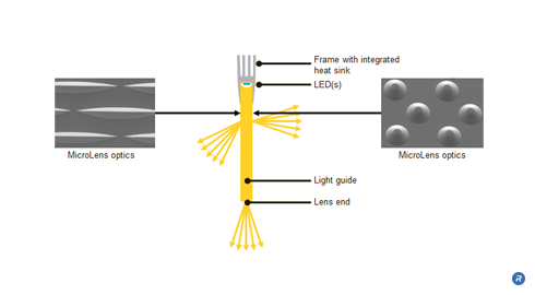
Fixtures that use traditional free-space reflectors — those that allow light to travel through air — can be cumbersome and inefficient when producing high-intensity beams of light. As an alternative to free-space reflectors, SolidCore™ reflectors are compact optics that produce high-brightness, collimated beams ideal for high-powered spotlights. SolidCore™ Reflectors enable smaller, thinner and lighter-weight fixtures that can be white or multi-colored by combining reflectors using red, green and blue LEDs.

  • High-efficiency, molded reflectors
  • Up to 75% reduction in reflector size for equivalent beam angle
  • Produces tightly controlled, high-intensity beams ideal for spotlights
  • Adjustable light emission according to the radius of the optic

What are SolidCore™ Reflectors?

Traditional free-space reflector versus SolidCore™ reflector technology

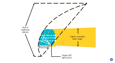
SolidCore™ Reflectors take advantage of the higher refractive index of plastic versus free space to produce a tighter angle of reflection. They are made of molded plastic, and unlike free space reflectors produce less variation in magnification and are far more compact. Each SolidCore reflector uses a single, high power LED. Light is directed to the reflective surface using a customized light pipe. The angle of the high-intensity, concentrated beam emitted by the SolidCore reflectors is determined by the radius of the optic. For example, beam output angles as tight as 3 degrees can be achieved with a 4″ radius optic.

Who Benefits?

With SolidCore reflectors, lighting designers are able to effects with much greater control, precision and intensity than ever before while maintaining power efficiency. The ability to control the beam angle and achieve color mixing delivers a richer and safer experience to consumers in multiple applications including entertainment, architecture, and outdoor lighting.

On Die Termination Calibration

As the performance requirements of digital systems continue to increase, there are increasing requirements to deliver signal integrity that enables reliable operation at higher signaling rates. Signal line terminations are useful elements in the management of signal integrity, and can be use external to the memory device or within the device itself. Incorporating a resistive termination within the DRAM device, which is often referred to as On Die Termination (ODT), improves the signaling environment by reducing the electrical discontinuities introduced with off-die termination. However, variations across process, voltage and temperature (PVT) can cause instability in the resistive characteristics of the ODT elements. Rambus ODT Calibration determines an optimal termination impedance to reduce signal reflections and compensate for variations across PVT.

  • Calibrates ODT termination impedance
  • Reduces signal reflections
  • Compensates for variations across PVT and operating conditions

What is On Die Termination Calibration Technology?

ODT Calibration Circuit

Conventional DRAM memory module architectures typically include line termination resistors on the motherboard. Although the termination resistors on the motherboard reduce some reflections on the signal lines, they are unable to prevent reflections resulting from the stub lines that connect to the DRAMs on the module. A signal propagating from the memory controller to the DRAM encounters an impedance discontinuity at the stub leading to the DRAM on the module. The signal that propagates along the stub to the DRAM will be reflected back onto the signal line, thereby introducing unwanted noise into the signal. The introduced noise and the consequential signal degradations that are not addressed by such off-die termination become more pronounced with higher data rates and longer stub lengths. Larger, multi-drop systems containing multiple DRAM modules introduce even more reflections and consequently add more reflective noise, thereby resulting in further signal degradation.

By placing the termination resistance on the die itself rather than the motherboard, the reflections resulting from discontinuities in the line are significantly reduced, thus producing a cleaner signal and enabling faster data rates.

On Die Termination

ODT calibration is a technique that involves calibrating the termination impedance in order to optimize the reduction of signal reflections. ODT calibration allows an optimal termination value to be established that compensates for variations in process and operating conditions.

A calibrated ODT value significantly reduces unwanted signal reflections while only minimally attenuating the magnitude of the signal swing due to the added resistive loading. The resulting cleaner data signal allows for higher data rates.

ODT calibration is achieved by establishing an ODT impedance that is proportional to an external precision resistor. The same external resistor can also be used for Output Driver Calibration.

The ODT calibration controller, compares the voltage drop across the ODT resistor network with a voltage drop across an external resistor represented. The controller modifies the resistor network with coarse tuning and fine tuning to achieve an impedance value that closely approximates the external, reference resistance.

Who Benefits?

ODT calibration delivers benefits at the device, subsystem and system level. By implementing ODT calibration, devices are able to achieve enhanced signal performance and higher data rates, which enables designers to achieve superior DRAM device and module performance.

In addition, placing the termination components on the DRAM devices removes these elements from the PCB. In doing so, the number of components and signal lines on the motherboard is reduced, lowering the cost and complexity while increasing reliability.

Finally, the system benefits from the superior data rates and module performance that are enabled through the improved signal integrity achieved with ODT calibration.

MicroLens® Optics

The introduction of LEDs to the application of general lighting presents lighting architects and fixture designers with unprecedented capabilities unachievable with the constraints of bulb and fluorescent tube-based luminaires. In addition to lower cost, lower energy consumption, and greater control and directionality of light, LEDs offer tremendous freedom of design. However, as point sources of light, LEDs have introduced a new challenge of delivering uniform, controlled light while maximizing the efficiency of fixtures and lamps. MicroLens® optics are 3-dimensional elements embedded in optical light guides to provide customizable control of the uniformity and distribution of light. When utilized in edge-lit architectures for LED-based fixtures and lamps, MicroLens® optics provide a cost-effective, high-efficiency solution for unmatched design possibilities.

  • Customizable control of light output uniformity and distribution
  • Up to 95% optical efficiency
  • Enable ultra-thin form-factors with unmatched freedom of design
  • Proven, low-cost manufacturing process

What are MicroLens Optics?

Custom ray angle control with MicroLens® Optics

MicroLens® optics are 3-dimensional elements that are embedded in an optical waveguide or film, that provide customizable control of uniformity and output ray angle distribution for superior application efficiency. Through the use of proprietary optical modeling software and design techniques, the MicroLens features and their pattern can be customized to efficiently spread the light across the entire lighting surface, or direct it in specific locations.

When combined with Rambus’ TruEdge™ LED coupling technology in edge-lit applications, MicroLens optics enable 92-95% optical efficiency in ultra-thin form factors with an unmatched freedom of design. Leveraging proven and low-cost manufacturing processes, MicroLens® optics provide a cost effective, high performance and low risk solution for lighting fixtures and lamps.

MicroLens® optical features are embedded directly into the light guide using injection molding, extrusion, or hot embossing processes. With advanced modeling techniques, the depth, shape and density of the MicroLens® features can be optimized to support a broad range of lighting solutions. Light injected at the edge of the light guide is precisely directed using the custom design of the MicroLens® optics.

Who Benefits?

When implemented in an edge-lit architecture, MicroLens® optics deliver tremendous flexibility of form factor and freedom of design without sacrificing efficiency or control. This will enable designers to create a new age of beautiful and functional lighting. The increased efficiency and control delivered by MicroLens optics translates to fewer fixtures and lamps required to deliver the desired amount of light and lower energy consumption and cost.

Consumers can reap the benefits of the cost-effectiveness of MicroLens through broad availability of reliable and affordable LED lighting solutions that deliver on the promise of green lighting technology.

Micro-Threading Technology

Improvements in DRAM interface throughput have rapidly outpaced comparable improvements in core speeds. Whereas data rates of DRAM interfaces have increased by over an order of magnitude over successive generations, the DRAM core frequency has remained relatively constant. Over time, core prefetch size has increased in order to keep pace with improvements in interface bandwidth. However, larger prefetch sizes increase access granularity—a measure of the amount of data being processed—and deliver more data than necessary, causing processing inefficiencies. Micro-threading is a unique DRAM core access architecture that improves transfer efficiency and effective use of DRAM architecture resources by reducing row and column access granularity. By providing independent addressability to each quadrant of the DRAM core, micro threading allows minimum transfer sizes to be four times smaller than typical DRAM devices, complementing the threaded memory workloads of modern graphics and multi-core processors. This unique architecture enables micro-threading to maintain the total data bandwidth of the device while reducing power consumption per transaction.

  • Improves transfer efficiency for multi-core computing applications
  • Doubles DRAM core data rate versus conventional techniques
  • Maintains high sustained bandwidth while lowering power consumption

What is Micro-threading Technology?

Typical 8-bank DRAM core

Access granularity is a function of the accessibility of data within a memory architecture. A typical DRAM is comprised of eight storage banks. Within such DRAMs, each bank is typically further subdivided into two half banks, “A” and “B”. For such a DRAM with 32 data pins, each A half bank is connected to 16 data pins and each B half bank is connected to 16 pins. The banks are in opposite quadrants of the physical die, and each quadrant has its own dedicated row and column circuitry – each bank half operating in parallel in response to the row and column commands.

A row command selects a single row in each bank half of the bank being addressed, thereby sensing and latching that row. Physical timing constraints impose a delay (i.e., tRR) before a row in another bank can be accessed. Column commands are similarly constrained (i.e., tCC). However, the row timing interval is typically twice the column timing interval; therefore two column commands can be issued during the mandatory delay required for a single row activation.

The column prefetch length, the amount of data delivered per transaction, is determined by the respective column and row timing delays and bit transfer rate, where:

Prefetch = timing delay/bit transfer rate

A core of a mainstream DRAM typically operates up to 200MHz, whereas a core of a high performance industry standard DRAM can typically operate up to 400MHz. Core frequencies exceeding 400MHz are difficult to achieve using modern industry standard DRAM technologies without sacrificing production yields or increasing costs. Therefore, a column prefetch of 16bit is required for such a high performance DRAM core to support external data rates exceeding 3200 MHz since the DRAM cores is organized with each half-bank operating under the same row or column operation

In addition:

Column granularity = (column prefetch) x (number of data pins per half bank) x (number of half banks per access)

Or:

For a 32-bit wide DRAM with 16 data pins per half bank:

Column granularity per access = 16 x 16 x 2 = 512 bits or 64 bytes.

Moreover, during the row timing interval, in order to maintain peak bandwidth, at least two column operations must be performed. This is typically described as two column address strobes per row address strobe (two CAS per RAS). This results in a minimum row granularity of 128 bytes. This large access granularity translates into inefficient data and power utilization for applications such as 3D graphics.

Micro-threaded 16-bank DRAM core

Using largely the same core resources as in the previous example, a sample micro-threaded DRAM core has 16 banks, each bank in the micro-threaded DRAM being equivalent to a half bank in the typical DRAM core. The even numbered banks connect to the A data pins and odd numbered banks connect to the B data pins (again with 16 pins in each case). However, unlike a typical core, each four-bank quadrant can operate independently, through the use of independent row and column circuitry for each quadrant. Moreover, interleaving, simultaneous access to more than one bank of memory, allows concurrent accesses to the lower quadrant on the same physical side of the core as the previous access.

Micro-threading enables four independent accesses to the DRAM core simultaneously. Although the same time interval as a typical core must still elapse before accessing a second row in a particular bank or bank quadrant, the three banks in the other quadrants remain separately accessible during the same period. Columns in rows in other quadrants can be concurrently accessed even though a column timing interval must pass before a second column is accessible in the previously activated row. The net effect of this quadrant independence and interleaving is that four rows (one in a bank of each quadrant) and eight columns (two in each row) are accessed during the row timing interval (compared to a single row and two columns with the typical DRAM technique).

Timings are similar to the typical DRAM core, but each column only sends data for half the column timing interval. The interleaved column sends data for the other half of the interval. Micro-threading reduces minimum transfer granularity size while maintaining a high-yielding and cost effective core frequency. By interleaving the column accesses from four different banks, a micro-threaded DRAM core (of a given column prefetch length and core frequency) can support data rate two times higher than that of a conventional DRAM core. Conversely, micro-threading of the column operation enables a DRAM core to cost-effectively sustain a specific data transfer and granularity while relaxing the column cycle time (tCC) by up to two times compared to those of a conventional DRAM core.

Micro-threaded data access optimization

With micro-threading, column granularity is now:

Column prefetch/2 x 16 pins = 16/2 x 16 = 128 bits or 16 bytes (one quarter of the previous value).

The row granularity is 32 bytes (again one quarter of the previous value). Micro-threading’s finer granularity results in a performance boost in many applications. For example, in a graphics application with 8 byte micro-threaded column access granularity, computational and power efficiency increased from 29 percent to 67 percent after introducing the technique.

Who Benefits?

Micro threading enables twice the data rate from a DRAM core over conventional techniques, providing memory system designers high sustained bandwidth while lowering power consumption. In addition, micro threading benefits DRAM designers and manufacturers by providing an alternative approach to improve efficiency and reduce access granularity using largely the same DRAM core, reducing cost and risk.

Fully Differential Memory Architecture

As data rates continue to increase, signal and power integrity are increasingly difficult to maintain in memory systems with single-ended signaling topologies. To enhance signal integrity and noise immunity across all communications between the memory PHY and the DRAM devices, Rambus implemented a Fully Differential Memory Architecture (FDMA) using a point-to-point topology, for data, clock, and command/address (C/A) channels. FDMA inherently reduces interference noise from simultaneous switching outputs (SSO) and crosstalk. Further, it reduces the EMI that would otherwise be generated in a single-ended system operating at the same data rate or frequency. With these advantages, FDMA enables very high-speed data transmission supported by full-speed operation of C/A channels.

  • Enables low-power, high-performance memory systems
  • Simplifies system design
  • Increases system reliability through improved noise immunity

What is a Fully Differential Memory Architecture?

Fully Differential Memory Architecture example - Differential signaling circuit diagram

Differential signaling uses two wires for each signal (bit). A complementary signal is transmitted on one line or the other using a small DC current. The current is passed through a resistor on each line to generate a voltage, the difference being measured at the receiver. Depending on the polarity, the signal is interpreted as a “1” or “0”. SSO noise, a function of the cumulative value of the total amount of current change, is reduced because the same amount of current is generated regardless of the bit’s value.

A further advantage of differential signaling is that for a given voltage at the transmitter, twice the voltage difference is measured at the receiver (the difference in voltage between the two wires in the current loop). This compares with single-ended signaling that exhibits the same voltage at the transmitter and receiver (the difference between the voltage on the wire and ground). Twice the voltage at the receiver means it takes twice as much noise to exceed the threshold of a valid voltage level.

In addition, differential signaling has superior noise immunity when compared to single-ended signaling due to its inherent common mode noise rejection. Any voltage noise that couples into one wire of a pair is likely to couple into the other. Because the difference between the two signals is measured at the receiver, the common noise components are effectively cancelled out. In addition to being less susceptible to noise, differential signal pairs create less EMI than single-ended signals. This is because changes in signal level in the two wires create opposing electromagnetic fields that superimpose and cancel each other out, reducing crosstalk and spurious emissions.

Who Benefits?

FDMA offers a scalable architecture for delivering memory system bandwidth performance up to and beyond one terabyte per second. It supports a lower operating power at any given data rate since lower voltage levels than those required in a single-ended system can be used to maintain sufficient signal integrity. Further, FDMA simplifies overall system design and increases reliability by harnessing differential signaling advantages of superior noise immunity and lower EMI generation.

Fly-by Command Address

Conventional, low-speed DRAM systems distribute clock, command, and address signals to multiple DRAMs using a topology in which those signals propagate to all of the DRAMs in the system at approximately the same time. In such systems, the propagation delays on the command and address lines introduce timing skew into the system, thereby limiting the operating frequency of the bus and ultimately impacting the performance of high speed memory systems. In addition, the performance of these topologies is also limited by capacitive loading. Both the flight time skew problem and the capacitive loading issues discussed above through the use of the Fly-by architecture. Fly-by command/address architectures improve signal integrity in memory systems, thus enabling higher per-pin bit rates and systems capable of GHz data rates while maintaining low latency, and avoiding the need for clock-encoding.

  • Improves signal integrity and overall system performance
  • Simplifies system design with relaxed timing constraints

What is Fly-by Command Address Technology?

Portion of the data eye taken up be the “flight-time skew”

Although the skew in the clock, command, and address arrival times at each DRAM is small, the skew becomes significant as clock frequencies continue to increase. In such systems, the frequency limitations on the Command /Address (C/A) bus that result from the skew become a limiting factor in trying to achieve reliable GHz-speed memory operation performance.

The variability in flight time from the memory controller to the memory devices, or “flight time skew”, can become a significant factor in high frequency systems with short clock periods. As shown, the flight time skew can consume a large portion of the available cycle time such that when operating at speeds greater than 1 GHz, very little time is left for reliable signal set-up and hold times. The issue is further compounded when operating at double data rates.

In trying to address the problem of flight time skew, a common solution is to try to match the trace lengths of the signal lines used to convey the command and address signals. One technique that tries to do such trace matching relies on a forked topology. In a forked topology, such as that illustrated below, the command, address, and clock signal traces are routed to a central node and then distributed from the central node to the individual DRAMs. By providing a signal distribution point closer to the DRAMs, the potential variability in trace length is limited to the shorter paths from the central node to the individual DRAMs.

Timing skew associated with a forked topology

Additionally, the performance of conventional DRAM topologies is constrained by capacitive loading. Adding memory devices to increase memory capacity on the module increases the capacitive loading of the C/A lines, thereby limiting the signaling rate on the C/A line.

Rambus patented innovations address both the flight time skew problem and the capacitive loading issues discussed above through the use of the Fly-by architecture. The Fly-by architecture was incorporated in Rambus DRAM systems as a means to enable increased memory capacity without impacting memory data rates. The Fly-by architecture optimizes the system transmission topology, is tolerant of timing skews and, when used in combination with FlexPhase™ circuit technology, can further manage any skew issues. Fly-by enables point-to-point data lines with scalable capacity without compromising memory data rates.

Timing skew addressed with Fly-by topology

In the Fly-by architecture the clock, address, and command are transmitted source synchronously to the DRAMs. As shown in the figure above, the clock signal propagates with the address and control information such that those signals arrive together at the interface of each DRAM. However, in this topology, the set of signals propagating on those lines arrives at each DRAM at a slightly different time. As can be seen from the illustration above, the signals will arrive at DRAM 1 shortly before DRAM 2 and so on. Because the arrival times of the signals at the DRAM interfaces are distributed in time, the time at which the signals encounter the input capacitance of each of the DRAMs is similarly distributed, thus reducing the capacitive loading issues discussed above. The reduced capacitive loading enhances the signal integrity and enables higher data rate signaling.

Further increases in data rates can be achieved by employing FlexPhase circuit technology to the data signals at the memory controller. Because the arrival times of the control and address signals at the DRAMs are distributed in time, the resulting data traffic received from the DRAMs on the separate data lines will also be slightly skewed in time. FlexPhase circuitry can be used to de-skew these incoming data signals. FlexPhase circuitry can also be used to pre-skew the data signals driven from the controller to the DRAMs so the data arrives with a well understood timing relationship with respect to the command and address signals.

The Fly-by Command Address architecture can also use routing traces on the circuit board that are terminated in order to achieve better controlled impedance on the line than would be realized using other topologies. Additional impedance mismatch reduction can be achieved by having shorter stub lengths from the command/address line to each DRAM device on the memory module. The improved impedance characteristics of the signal lines results in smaller signal reflections and less noise, which in turn enables higher frequency signaling.

Fly-by Command Address example - System employing Fly-by topology

In addition to providing higher data rates, another significant advantage of the Fly-by approach is that it is highly scalable in that multiple additional DRAMs can be inserted in a system to meet the needs of the relevant applications. With the added DRAMs, the Fly-by architecture is able to maintain high data rates on the Command/Address/Clock signals, whereas other topologies are limited by flight time skew, capacitive loading and impedance mismatches. Such non-Fly-by topologies often must reduce signaling rates on the Command/Address lines to accommodate the added DRAMs, thereby reducing system performance.

When used with FlexPhase circuit technology, the Fly-by architecture allows designers to relax PCB trace length requirements because the timing variations can be managed on the memory module with the FlexPhase circuit technology. Rambus has also developed Dynamic Point to Point technologies that, when used in combination with Fly-by, enable memory upgrades while maintaining bandwidth.

Who Benefits?

Fly-by architectures enable subsystems that require operational data rates that are significantly greater than those achievable with conventional approaches. Using Fly-by architectures allows designers to relax PCB trace length requirements allowing much simpler and more compact memory sub-system layouts.

In addition, Fly-by architectures provide system benefits by enabling DRAM systems to operate with GHz data rates. This superior DRAM system performance results in improved performance in desktops, notebooks, enterprise servers and storage, HDTVs, gaming systems, and handheld portable devices for end users.

  • « Go to Previous Page
  • Go to page 1
  • Go to page 2
  • Go to page 3
  • Go to page 4
  • Go to page 5
  • Go to Next Page »

Footer

About

  • Corporate Overview
  • Leadership
  • Careers
  • Locations
  • Investor Relations
  • News
  • Corporate Responsibility

Products

  • Memory PHYs
  • SerDes PHYs
  • Digital Controllers
  • Server DIMM Chipsets
  • Root of Trust Solutions
  • Provisioning and Key Management
  • Protocol Engines
  • Crypto Accelerator Cores
  • Software Protocols
  • DPA Countermeasures
  • Anti-Counterfeiting
  • CryptoMedia

Markets

  • AI & Machine Learning
  • Automotive
  • Data Center
  • Edge
  • Government
  • IoT
  • Pay TV

Resources

  • Resource Library
  • Webinars
  • Inventions
  • Buying Guide
  • Contact

Copyright © 2022 Rambus.com. All Rights Reserved. Privacy Policy | Trademark & Guidelines

  • Facebook icon
  • Twitter icon
  • YouTuve icon
  • LinkedIn icon
  • Blog icon