• Skip to primary navigation
  • Skip to main content
  • Skip to footer
  • English
  • Investor Relations
  • Resource Library
  • Newsroom
  • Blog
  • Careers
  • Support Center
Rambus Logo

Rambus

At Rambus, we create cutting-edge semiconductor and IP products, spanning memory and interfaces to security, smart sensors and lighting.

  • Products
      • All
          • Memory Interface Chips
          • DIMM Chipsets
          • DDR5 DIMM Chipset
          • DDR4 NVRCD
          • DDR4 Register Clock Driver
          • DDR4 Data Buffer
          • CXL Memory Interconnect Initiative
          • Interface IP
          • Memory PHYs
          • GDDR6 PHY
          • HBM3 PHY
          • HBM2E PHY
          • DDR4 PHY
          • More…
          • SerDes PHYs
          • PCIe 6.0 PHY
          • PCIe 5.0 PHY
          • 32G C2C PHY
          • 32G PHY
          • 28G PHY
          • More…
          • Digital Controllers
          • Memory Controllers
          • CXL & PCI Express Controllers
          • MIPI Controllers
          • Video Compression and Forward Error Correction Cores
          • Security IP
          • Root of Trust Solutions
          • Security Protocol Engines
          • Inline Cipher Engines
          • Crypto Accelerator Cores
          • DPA Countermeasures
          • Software Protocols & Crypto Toolkits
          • Anti-Counterfeiting
          • Provisioning and Key Management
      • Memory Interface Chips
        • DIMM Chipsets
          • DDR5 DIMM Chipset
          • Non-Volatile DDR4 Registering Clock Driver
          • DDR4 Register Clock Driver
          • DDR4 Data Buffer
          • DDR3 Register Clock Driver
          • DDR3 Isolation Memory Buffer
        • CXL Memory Interconnect Initiative

        • Made for high speed, reliability and power efficiency, our DDR3, DDR4, and DDR5 DIMM chipsets deliver top-of-the-line performance and capacity for the next wave of computing systems. Learn more about our Memory Interface Chip solutions
      • Interface IP
          • Memory PHYs
            • GDDR6 PHY
            • HBM3 PHY
            • HBM2E PHY
            • DDR4 PHY
            • DDR4 Multi-modal PHY
            • DDR3 PHY
          • SerDes PHYs
            • PCIe 6.0 PHY
            • PCIe 5.0 PHY
            • PCIe 4.0 PHY
            • 32G C2C PHY
            • 32G PHY
            • 28G PHY
            • 16G PHY
            • 12G PHY
            • 6G PHY
          • Digital Controllers
            • HBM3 Controller
            • HBM2E Controller
            • GDDR6 Controller
            • LPDDR5 Controller
            • CXL 2.0 Controller
            • PCIe 6.0 Controller
            • PCIe 5.0 Controller
            • MIPI CSI-2/DSI-2 Controllers
            • Video Compression and Forward Error Correction Cores
            • More…

        • With their reduced power consumption and industry-leading data rates, our line-up of memory interface IP solutions support a broad range of industry standards with improved margin and flexibility. Learn more about our Interface IP solutions
      • Security IP
          • Root of Trust Solutions
          • Security Protocol Engines
            • MACsec Engines
            • IPsec, TLS, SSL Multi-Protocol Engines
            • High Speed Public Key Accelerator
          • Inline Cipher Engines
          • Crypto Accelerator Cores
            • DPA Resistant Cores
            • Basic Crypto Blocks
          • Anti-Counterfeiting
            • CryptoFirewall Cores
            • Circuit Camouflage Technology
          • DPA Countermeasures
            • DPA Resistant Cores
            • DPA Resistant Software Libraries
            • DPA Workstation Platform
          • Software Protocols & Crypto Toolkits
            • IPsec Toolkit
            • FIPs Cryptographic Libraries
            • MACsec Toolkit
            • IoT Security Framework
          • CryptoMedia
            • Content Protection Core
            • Content Protection Services
          • Provisioning and Key Management
            • CryptoManager Provisioning
            • CryptoManager Device Key Management

        • From chip-to-cloud-to-crowd, Rambus secure silicon IP helps protect the world’s most valuable resource: data. Securing electronic systems at their hardware foundation, our embedded security solutions span areas including root of trust, tamper resistance, content protection and trusted provisioning. Learn more about our Security IP offerings
  • Markets
      • AI & Machine Learning
        • Speed and Security for the Artificial Intelligence & Machine Learning Revolution
          • Products
          • SerDes PHYs
          • Memory PHYs
          • Digital Controllers
          • Memory Interface Chips
          • Root of Trust
          • Crypto Accelerator Cores
          • Protocol Engines
          • Provisioning and Key Management
          • AI & Machine Learning
      • Automotive
        • Providing Performance & Security for the Connected Car
          • Products
          • Memory PHYs
          • SerDes PHYs
          • Digital Controllers
          • Root of Trust
          • PKE Engine
          • MACsec Engines
          • Crypto Accelerator Cores
          • Provisioning and Key Management
          • Explore Automotive
      • Data Center
        • Optimizing capacity, connectivity and capability of the cloud
          • Products
          • SerDes PHYs
          • Memory PHYs
          • Digital Controllers
          • Memory Interface Chips
          • Root of Trust
          • MACsec Engines
          • Software Protocols
          • Provisioning and Key Management
          • See Data Center
      • Edge
        • Catching a tidal wave of data
          • Products
          • Memory PHYs
          • SerDes PHYs
          • Digital Controllers
          • Root of Trust
          • Crypto Accelerator Cores
          • Protocol Engines
          • Software Protocols
          • Discover Edge
      • Government
        • Securing Mission-critical Systems
          • Products
          • Root of Trust
          • Protocol Engines
          • Anti-Tamper Cores
          • Provisioning and Key Management
          • DPA Workstation Platform
          • SerDes PHYs
          • Memory PHYs
          • Digital Controllers
          • See Government
      • IoT
        • Making IoT Data Safe & Fast
          • Products
          • Root of Trust
          • TLS Toolkits
          • Provisioning and Key Management
          • Memory PHYs
          • SerDes PHYs
          • Digital Controllers
          • Explore IoT
  • Resources
    • Inventions
    • Buying Guide
    • Resource Library
      • Webinars
      • Product Selector
  • About
      • Corporate Overview
      • Leadership
      • Inventors
      • Careers
      • Locations
      • Investor Relations
      • Newsroom
      • Blog
      • Events
      • Partnerships
      • Certifications
      • Corporate Responsibility
      • Contact
Home > Inventions > Page 4

Inventions

FlexMode™ Interface

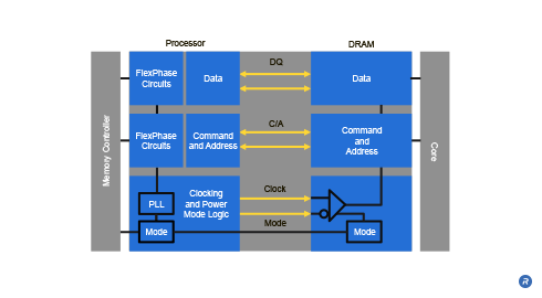
As chip design and fabrication costs continue to rise with each new process node, the ability to integrate flexible, cost-effective multi-purpose interfaces becomes increasingly valuable. Traditional multi-modal implementations combine the worst-case signal pin count for the functional blocks of the interface for each memory type growing the pin count, area and cost of the interface with each mode supported. Rambus’ FlexMode™ Interface technology uses a programmable assignment of signaling pins as either data (DQ), or command/address (C/A), to enable multi-modal functionality while minimizing signal pin count, even when combining different signaling techniques such as single-ended and differential. This enables an SoC memory controller to be implemented in a single package design with no additional signal pin overhead. An SoC using FlexMode™ Interface technology can address a broad range of system requirements, from entry-level to high-end, without additional cost.

  • Supports multi-modal functionality– either single-ended or differential—in a single SoC, with no additional pins
  • Enables seamless transition to next-gen, high-performance, low-power memory
  • Delivers cost-effective flexibility for next-gen chip designs

What is FlexMode Interface Technology?

FlexMode™ Interface Technology

Traditional multi-modal implementations combine the worst-case signal pin count for the functional blocks of the interface for each memory type. When combining functionality of multiple memory types with differing signaling architectures, such as single-ended and differential, this implementation technique can lead to costly design inefficiencies including increased pin count and costs.

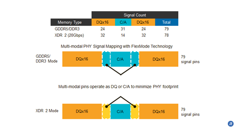
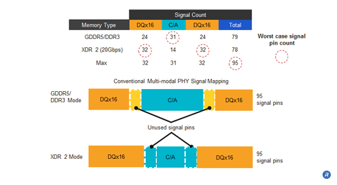
As an example, conventional signal mapping for a 32-bit wide single-ended DDR3 and GDDR5 memory interface combined with a differential XDR™2 memory interface would combine the 64 DQ pins from the XDR 2 memory (worst case DQ) and the 31 C/A pins from the DDR3 interface (worst case C/A) for a total of 95 signal pins (see “Conventional Multi-Modal Interface” diagram). This translates to a 16 signal pin overhead versus the single-ended GDDR5/DDR3 interface.

Conventional multi-modal interface

Who Benefits?

Rambus’ FlexMode™ Interface technology enables multi-modal functionality across differential and single-ended signaling memory types with no additional pin overhead and in a single SoC package design. By advancing data rates to up to 20 gigabits per second in an extremely power-efficient way with XDR 2 memory, and enabling compatibility to current industry-standard memories including GDDR5 and DDR3, FlexMode interface technology removes the technical and business barriers for customers to achieve unprecedented capabilities in their products.

Commercial server managers and consumer end users benefit from the reduced cost of ownership and increased battery life for their end systems and devices.

FlexLink™ C/A Interface

Traditional industry-standard memory architectures use wide, single-ended command/address (C/A) channels that operate at a considerably lower frequency than the data rate of the system. These wide, multi-drop interfaces require more pins and have greater power requirements. Given the pin and area requirements, scaling of wide busses becomes increasingly impractical. FlexLink™ C/A interface is a full-speed, differential, point-to-point C/A interface technology that provides flexible access granularity and scalable capacity. Using this innovation, the C/A channel can be implemented with as a little as two wires per DRAM device, reducing area, power, pin count, and overall system costs.

  • Provides capacity and access granularity scalability at reduced system costs
  • Reduces area, power and pin count on DRAM and controller interfaces
  • Enables memory system operation up to 20Gbps

What is FlexLink C/A Interface Technology?

FlexLink™ C/A interface

The industry’s first full-speed, scalable point-to-point command/address channel, FlexLink C/A provides the command and address information to a DRAM using a single, differential high speed communications channel. Unlike wide, single-ended C/A channels, narrow FlexLink C/A channels operating at the full-speed of the data, provide a straightforward path for scaling of capacity and access granularity.

Capacity scalability with FlexLink™ C/A interface

An example is a memory system using four independent FlexLink C/A channels and 32 data (DQ) links supporting 32-byte access granularity. Such a system can support one, two or four DRAM devices, allowing for scaling of capacity while maintaining system bandwidth and 32-byte access granularity. Similarly, the FlexLink C/A interface supports scalable access granularity by increasing the number of C/A links per DRAM. For example, a controller attached to a single DRAM through one, two or four independent C/A channels and 32 DQ links would support 128-, 64- or 32-byte access granularity, respectively.

Access granularity scalability with FlexLink™ C/A interface

Who Benefits?

FlexLink C/A interface technology enables memory systems operating at up to 20Gbps and providing upwards of a terabyte per second of bandwidth. It minimizes the controller area and number of pins required to implement the C/A channels. With lower pin counts, and lower voltages thanks to differential signaling, FlexLink C/A reduces overall interface power and costs for DRAM and controller designers. Given the robust signaling characteristics of differential signaling, FlexLink C/A increase system reliability. In addition, FlexLink C/A provides designers great flexibility through a straightforward means to scale memory system capacity and access granularity.

FlexClocking™ Architecture

Traditional, multi-gigahertz memory interfaces require timing synchronization circuitry in both the controller and memory interface in order to compensate for any skew that arises between clock, data, and command/address (C/A) signals. FlexClocking™ Architecture technology is an architecture that utilizes asymmetric partitioning and places critical calibration and timing circuitry in the controller interface, greatly simplifying the design of the DRAM interface. The clock is forwarded and distributed to both the controller circuit blocks and the DRAM device from a central PLL located in the memory controller interface (PHY).

  • Reduces DRAM power consumption
  • Simplifies DRAM interface design
  • Enables fast power state transition times
  • Eliminates PLL or DLL on DRAM

What is FlexClocking Architecture Technology?

FlexClocking™ Architecture with Advanced Power State Management

This architecture features the use of a single clock multiplier where the DRAM interface operates in a single, high-speed clock domain derived from a half-bit-rate clock forwarded from the controller. The command/address (C/A) and data (DQ) links are implemented as bi-directional differential serial transceivers with 8:1 multiplexing. A peak interface bandwidth of greater than 17GB/s can be achieved using only four bytes of DQ links operating at 4.3Gbps, 8 C/A links, and a single forwarded clock operating at 2.15GHz.

Given this unique topology, the FlexClocking™ Architecture enables high-speed operation without the need for a DLL or PLL on the DRAM device. This is made possible in part by the Rambus FlexPhase™ technology which is used to adjust for any variability between the clock and DQ signals received at the DRAM device. As a result, DRAM design is simplified and power consumption is significantly reduced.

Who Benefits?

FlexClocking™ Architecture enables high-speed operation in a memory system without the need for a PLL and/or DLL on the DRAM, reducing complexity and cost for DRAM designers. In addition, it allows for fast transition times from low-power to active modes and superior power efficiency delivering enhance response times and increased battery life to end users.

Enhanced FlexPhase™ Timing Adjustments

In memory architectures, it can be used to deskew data bits inbound to the controller (Reads) in order to compensate for uncertainty in the arrival times of signals. Enhanced FlexPhase™ circuits implemented in a memory controller finely tune the timing relationships between data, command and address (C/A), and clock signals to eliminate the need for trace length matching in systems operating up to 20Gbps. Further, Enhanced FlexPhase circuits can inject a timing offset, or “preskew,” such that the data outbound from the controller (Writes) arrives at the DRAM devices coincident with the C/A signals.

  • Eliminates trace length matching on system boards and memory devices packaging at speeds up to 20Gbps
  • Reduces board and packaging costs
  • Enables timing calibration at extremely high signaling rates

What is Enhanced FlexPhase Technology?

Enhanced FlexPhase technology anticipates the phase difference between signals on separate traces and manages the transmission of bits so that data arrives with a known timing relationship with respect to the C/A signal. It can also adjust for differences in signal propagation times due to manufacturing variations in trace lengths. Building on the foundation of FlexPhase technology, Enhanced FlexPhase technology adds:

  • New circuit innovations to increase phase linearity and tighten timing resolutions to support data rates of up to 20Gbps
  • Innovative timing calibration algorithms for optimizing phase settings of C/A signals at initialization and in active operation
  • Methods to statistically measure bit error rate (BER) at low enough magnitudes to account for all deterministic jitter (DJ) sources
  • Ability to measure BER during characterization of the memory system

Enhanced FlexPhase circuits include in-system timing characterization and self-test functionality that enables extremely fine timing resolutions in high-performance memory systems. Enhanced FlexPhase technology incorporates calibration algorithms that establish communication of the C/A signal and accelerate the search for the optimal phase value. In active operation, Enhanced FlexPhase circuits can also periodically fine-tune the timing of the C/A signals without disturbing the operational state of the DRAMs.

Who Benefits?

Enhanced FlexPhase technology eliminates the need to match trace lengths both on system circuit boards and within memory device packages. Such system simplification allows greater flexibility and lowers board and packaging costs. It also improves overall system timing through dynamic compensation for process variations, on-chip clock skew, driver/receiver mismatch and clock standing wave effects. Enhanced FlexPhase technology delivers these system benefits even at extremely high signaling rates up to 20Gbps.

Dynamic Point-to-Point

As the performance demands of personal and enterprise computing continue to rise, memory system designers are challenged to meet the memory speed and capacity requirements needed to address the growing demand. The traditional method of supporting memory system capacity expansion is through the use of a memory bus with a multi-drop topology, which supports multiple devices per data signal. These topologies support upgradeability and multiple modules per memory bus, but can degrade signal integrity and ultimately, the speed the of the memory bus. Point-to-point topologies, which support one device at each end of the signal line, have better signal integrity properties and permit higher bus speeds, but cannot be upgraded with multiple modules. Dynamic Point-to-Point (DPP) technology combines the benefits of multi-drop and point-to-point topologies by enabling upgrade in capacity without degrading signal integrity and memory bus speed.

  • Enables capacity expansion at full memory bandwidth
  • Support for multiple modules at data rates up to 6.4Gbps
  • Dynamically configures memory channel to support multiple modules with the same controller
  • Backwards compatible with most standard signaling such as SSTL and RSL

What is Dynamic Point-to-Point Technology?

Base memory system configuration: One 32-bit module installed

A key benefit of DPP technology is that by providing capacity expansion, DPP technology allows point-to-point upgrades at full memory system bandwidth. DPP technology can be applied to many different types of memory technologies, including DDR4 and beyond. In an example 32-bit DDR3 memory system, the base system configuration has a single memory module, with this module supplying all of the memory bandwidth across the full datapath width. A continuity module occupies the second memory slot, providing electrical continuity that maintains the point-to-point connection across half of the datapath.

When the continuity module is removed and an expansion module is added, the datapath is reconfigured to supply memory bandwidth from both modules. In this example, each module supplies half of the memory system bandwidth across a different half of the datapath in a point-to-point topology. Using DPP technology, the single 32-bit module is “dynamically rewired” to become a 16-bit module when the second module is added. In order to accomplish this the width of the memory devices on the module must change from x4 DRAMs to X2 DRAMs in the upgraded module configuration. In the x4 mode, each DRAM supplies four bits of data, two bits directly to the ASIC and two bits through the continuity module to the ASIC. When an upgrade module is inserted, the path through the continuity module is broken and the devices switch to x2 mode. In x2 mode, each DRAM supplies two bits of data directly to the ASIC.

Upgrade memory system configuration: Two 32-bit modules installed

Before and after the capacity upgrade, point-to-point signaling is maintained, allowing memory system bandwidth to be maintained. The dynamic rewiring in DPP technology allows the memory system to retain the signal integrity benefits of point-to-point signaling while enabling memory system capacity expansion at full memory system bandwidth. DPP technology can be used in conjunction with FlexPhase technology, together forming a compelling framework for memory system architecture.

Who Benefits?

DPP delivers benefits to system designers, integrators and consumers. The degraded signal integrity and overall memory speed cause by multi-drop topologies can cause significant challenges for system designers. The improved signal integrity that DPP technology provides frees memory bus speeds from multi-drop signaling constraints. DPP technology also allows system designers to increase memory capacity without sacrificing signal integrity. Like system designers, system integrators benefit from the improved signal integrity that DPP technology provides, allowing more robust systems to be created. Finally, consumers benefit from the increased data rates a module upgrades provided by DPP technology, enabling capacity expansion without sacrificing performance.

DLL/PLL on a DRAM

As CPU speeds continue to increase, memory performance becomes more of a limiting factor in system performance. For system performance to increase, memory performance must increase as well. An important aspect of increasing memory performance is increasing the speed at which data can be transmitted to and from the DRAMs in the memory system. In the early 1990s, Rambus designed the first DRAMs that incorporated DLLs and PLLs, important innovations that allowed DRAMs to achieve 500 MHz signaling rates, more than eight times faster than the prevailing DRAM communication rates at the time.

  • Maximizes operating frequency of a memory system
  • Increases DRAM performance
  • Improves DRAM yield and reduced production costs

What is DLL/PLL on a DRAM Technology?

Low and high-speed signaling without a DLL/PLL on a DRAM

Modern systems use synchronous communication to achieve high data transmission rates to and from the DRAMs in the memory system. Systems that communicate synchronously use a clock signal as a timing reference so that data can be transmitted and received with a known relationship to this reference. A difficulty in maintaining this relationship is that process, voltage, and temperature variations can alter the timing relationship between the clock and data signals, resulting in reduced timing margins. This problem gets worse as signaling speeds increase, limiting the ability of systems to communicate data at higher speeds.

Timing margins, in particular, can be affected by process, voltage, and temperature at low and high signaling speeds. At low signaling speeds (the left side of Figure 1), DataPVT1 illustrates the relationship of the data valid window (the time over which data can be reliably sampled by the receiver) and the clock for a given set of operating conditions. Likewise, DataPVT2 shows the relationship of the data valid window and the clock for a different set of operating conditions. These two sets of operating conditions represent the operational extremes over which the device functions. Receiver circuitry does not typically understand how the data valid window changes as process, voltage, and temperature change at the transmitter. Because of this, the receiver circuitry is designed to sample data within a window of time that data is valid across all allowed operating conditions. If DataPVT1 and DataPVT2 represent the soonest and latest (relative to the clock signal) data valid windows, then the receiver will assume a data valid window that is the intersection of these two, and choose a sample point within this resulting data valid window that is valid across process, voltage, and temperature variations.

At low signaling speeds, the data valid window (the time over which data can be sampled reliably by the receiver) can be large. Even in the presence of a substantial shift in the data valid window across operational extremes, the resulting data valid window can still be large enough to transmit and receive data reliably. This is the case for DRAM technologies such as SDRAM. However, for higher-speed DRAM technologies such as RDRAM and DDR, variations in process, voltage, and temperature can result in the loss of the data valid window. The right side of Figure 1 shows that at higher signaling speeds, the data valid windows for both DataPVT1 and DataPVT2 are smaller, reflecting the fact that information must be transmitted more quickly at higher signaling rates. Although the data valid windows are smaller, these windows still shift the same amount across process, voltage, and temperature (assuming no manufacturing improvements or changes in operating environment). Because these data valid windows are smaller, the resulting intersection of the data valid windows yields no resulting data valid window during which receiver circuitry can reliably sample data.

As process, voltage, and temperature vary, the timing characteristics of the output logic and output driver change, causing the data valid window to shift. In order to transmit and receive data at high speeds, this timing variation needs to be addressed.

DLL/PLL on a DRAM block diagram

Delay Lock Loops (DLLs) and Phase Lock Loops (PLLs) serve similar purposes, and can be used to maintain a fixed timing relationship between signals in environments where process, voltage, and temperature variations cause these relationships to change over time. DLLs and PLLs work by continuously comparing the relationship between two signals and providing feedback to adjust and maintain a fixed relationship between them. Rambus DRAMs were the first DRAMs to incorporate DLLs and PLLs, an important innovation that resulted in increased signaling speeds, compared to alternative DRAM technologies.

Maintaining timing with a DLL/PLL on a DRAM

A DLL is used to maintain the timing relationship between a clock signal and an output data signal. A critical element of the DLL is the phase detector, which detects phase differences between the clock and output data. The phase detector detects this phase difference, and sends control information through a low pass filter to a variable delay line that adjusts the timing of the internal clock to maintain the desired timing relationship (PLLs use a voltage controlled oscillator to adjust this timing relationship). One of the difficulties of maintaining phase relationships between these two signals is that the loop which provides feedback to the phase detector must account for the timing characteristics of the output logic and output driver. This is important, as it estimates the phase differences between the clock and the data being driven by the output driver. In order to accomplish this, circuits that mimic the behavioral characteristics of the output logic and output driver are inserted into this feedback loop to model timing delays and changes in behavior as process, voltage, and temperature vary. Maintaining the timing relationships between the clock and output data in this manner with DLLs and PLLs results in improved timing margins (as shown in Figure 4), and addresses an important limitation to increasing signaling speeds.

PLLs are similar to DLLs, but can also be used to divide-down or multiply-up an external system clock frequency for use in other parts of a chip. PLLs can be used to provide a slower clock frequency to the core of a DRAM, while the interface operates at a higher clock frequency. PLLs used in this manner enable DRAM core prefetch, allowing the DRAM core to operate at a slower frequency (improving DRAM yield), while allowing the interface to run at higher speeds to improve system performance.

High-speed signaling with a DLL/PLL on a DRAM

In 1993 Rambus published details of a 500 MHz PLL design at the International Solid State Circuits Conference (ISSCC), the premier conference on circuit design. One year later, Rambus published details of a 500 MHz DLL in a paper presented at ISSCC in 1994. Both papers received prestigious Best Paper awards in recognition of the groundbreaking innovations described in each.

Who Benefits?

End Users, DRAM manufacturers, designers and integrators can all benefit by incorporating a DLL/PLL on a DRAM. By providing a fixed timing relationship between clock and data signals, DRAM performance is allowed to increase and end users are able to benefit from the overall improvement in system performance. DRAM manufactures are able to reduce production costs and improve DRAM yields with the ability to adjust the timing relationships to compensate for variations in process, voltage and temperature, improving timing margins. By enabling high per-pin transfer rates, DLLs and PLLs allow controller and board designers to reduce IO pin counts, which decreases packaging costs, component count, routing area, and routing complexity. Finally, the ability of DLLs and PLLs to provide fixed timing relationships lets component manufacturers and system integrators relax the specifications. In systems with varying temperature and voltage characteristics, system thermal and power delivery requirements can be relaxed and the DRAMs can still maintain good timing margins, while lowering the costs of the thermal solution, power supply, and system manufacturing.

  • « Go to Previous Page
  • Go to page 1
  • Go to page 2
  • Go to page 3
  • Go to page 4
  • Go to page 5
  • Go to Next Page »

Footer

About

  • Corporate Overview
  • Leadership
  • Careers
  • Locations
  • Investor Relations
  • News
  • Corporate Responsibility

Products

  • Memory PHYs
  • SerDes PHYs
  • Digital Controllers
  • Server DIMM Chipsets
  • Root of Trust Solutions
  • Provisioning and Key Management
  • Protocol Engines
  • Crypto Accelerator Cores
  • Software Protocols
  • DPA Countermeasures
  • Anti-Counterfeiting
  • CryptoMedia

Markets

  • AI & Machine Learning
  • Automotive
  • Data Center
  • Edge
  • Government
  • IoT
  • Pay TV

Resources

  • Resource Library
  • Webinars
  • Inventions
  • Buying Guide
  • Contact

Copyright © 2023 Rambus.com. All Rights Reserved. Privacy Policy | Trademark & Guidelines

  • Facebook icon
  • Twitter icon
  • YouTuve icon
  • LinkedIn icon
  • Blog icon