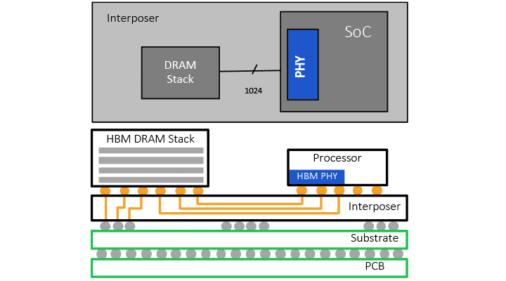
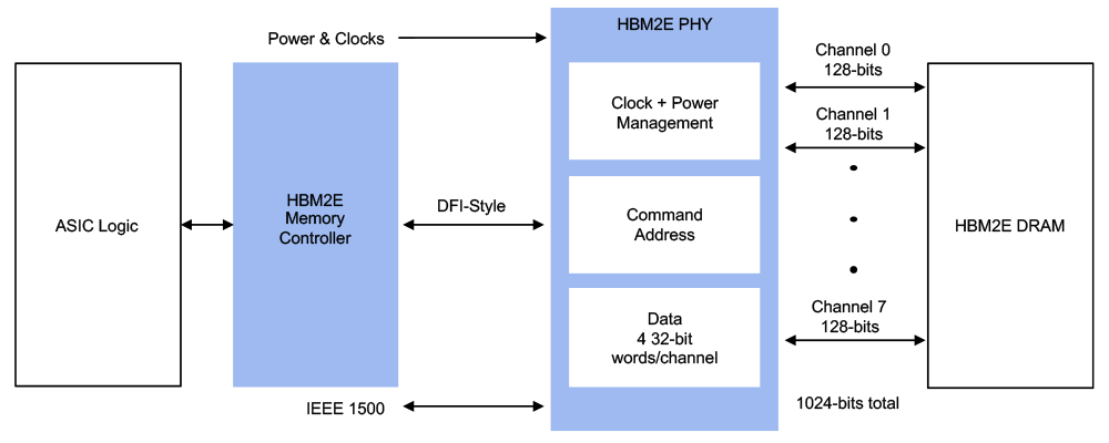
Rambus has announced a comprehensive interface solution for HBM2E memory consisting of co-verified PHY and memory controller. Operating at a top speed of 3.2 Gbps over a 1024-bit wide interface, the interface can deliver 410 GB/s of bandwidth with a single HBM2E DRAM stack.
Read first our primer on:
HBM2E Implementation & Selection – The Ultimate Guide »

In addition to the speed jump from 2.0 to 3.2 Gbps for HBM2E vs. HBM2, this latest iteration of the HBM standard now supports 12-high DRAM stacks of up to 24 Gb devices, providing an aggregate stack capacity of 36 GB. With 3D stacking of memory, HBM2E provides high bandwidth and high capacity at low power and low latency in a very small footprint.
For AI/ML, HBM2E delivers an outstanding combination of features. AI training capabilities are growing at 10X per year with rapidly expanding training set sizes. With AI/ML training running in data centers that are increasingly space and power constrained, HBM2E’s compact size and low power, in combination with its unmatched bandwidth and capacity, make it an ideal solution.

The Rambus co-verified PHY and controller greatly reduce integration complexity for chip designers. Both PHY and controller are fully compliant with the JEDEC JESD235B standard and are backward compatible to HBM2. While together they are an ideal complete solution, both PHY and controller can be paired with JESD235B-compliant 3rd-party solutions if so desired.
This latest portfolio addition highlights Rambus leadership in high-speed memory PHY and controller IP, leveraging the company’s long tradition of signal and power integrity expertise coupled with the design talent and products from recently acquired Northwest Logic. Get all the details on the HBM2E interface solution here.


Leave a Reply