In this two-part blog series based on a recent Semiconductor Engineering article, Rambus engineers Niall Sorensen and Malini Narayana Moorthi take an in-depth look at how to overcome high-speed SerDes IP integration challenges. In part one, the two point out that SerDes design is a complex process which requires a multidisciplinary team of analog, digital, and physical designers and software engineers, as well as support from silicon-validation and operations teams. Perhaps not surprisingly, it has become more time and cost effective to source SerDes from an IP vendor specializing in the technology.
The role of the SerDes IP vendor is to ensure the effective integration of its IP into the ASIC. However, SerDes IP vendors must deal with multiple challenges and issues during the integration process, including IP pin list and ensuring accurate design simulation (both topics are discussed in-depth in part one of this two-part blog series). SerDes IP vendors must also understand timing analysis/place and route, board/PCB design issues, bring-up readiness, as well as silicon compliance, debug, and failure analysis.
Timing Analysis/Place & Route
According to Sorensen and Moorthi, SerDes clock speeds in the digital layer are increasing to rates of 1Ghz and beyond. As data rates increase and bus widths remain steady, this is a natural progression. For example, PCIe Gen4 runs at 16Ghz with a 16-bit bus width and a 1Ghz clock speed.
“Higher speed clocks result in lower design latencies on the data path which is beneficial for communication speed over networks. However, this creates a challenge for timing closure with a SerDes design that can include a complex array of clock loopbacks and control blocks running at these transmit (TX) and receive (RX) clock speeds,” the two explain. “If the digital layer of the SerDes design is provided to ASIC integrator in a soft Verilog or VHDL format, the ASIC integrator is expected to synthesize, place and route (P&R) and close timing successfully on the design. Given that the ASIC integrator is generally not intimately familiar with the IP design, this can present a challenge.”
To successfully close timing, says Sorensen and Moorthi, Rambus provides the ASIC integrator with synthesis design constraints (SDC). Essentially, SDC offers a high-level description of the clocking scheme for the design including clock definitions, clock groups, clock frequencies, clock crossing domains, and non-standard clocking schemes. In addition, an application note is provided including detailed information on clock mux design, suggested clock tree timing budgets for the critical high-speed TX and RX data path, as well as instructions on clock balancing for loopback and mission mode clocking.
“For the analog portion of the design, Rambus provides liberty timing models for the analog front end (AFE) portion of the design that is a hardened custom transistor design,” the two elaborate. “The liberty timing model specifies the timing delays on the interface between the AFE and the digital layer. Rambus also supports annotated gate-level simulations to catch any functional timing issues that may not be caught using static timing analysis (STA) tools.”
Board/PCB Design Issues
As data rates increase, board design becomes increasingly challenging. This means a wide range of factors must be taken into consideration when designing a PCB board and package including:
- Crosstalk
- Impedance matching
- Intra-channel skew
- Supply decoupling
- Insertion/return loss
- Regulator supply noise
- Connector choice
This is precisely why Rambus provides a detailed application note with instructions and specifications for the ASIC integrator to have signoff criteria for all the aspects of channel and noise quality outlined above.
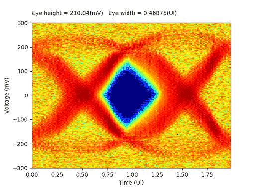
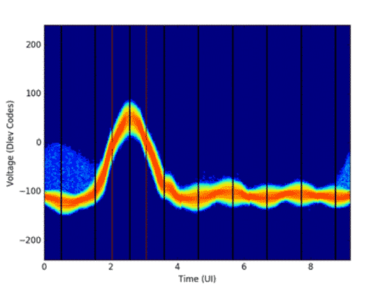
“Although many ASIC integrators are very knowledgeable of high-speed board and package design, and while outside the design of the SerDes IP, it is always helpful to provide clear instructions to avoid these kinds of issues,” Sorensen and Moorthi state. “In addition, Rambus provides several debug tools as part of the IP to analyze signal integrity (SI) and channel related issues, including an eye diagram and an impulse response analyzer to find channel reflections, crosstalk, etc.”

Figure 1 Example Eye Diagram (Rambus)

Figure 2 Example Impulse Response Diagram (Rambus)
Bring-Up Readiness
According to Sorensen and Moorthi, there are many questions that should be answered when a chip finally comes back to the ASIC integrator’s lab. This is because there is typically a lull of several months between the tape out and the chip’s return. These questions include:
Do/did you:
- Have the equipment you need to bring up the design?
- Conduct a full package and board review to remove SI surprises?
- Run system simulations?
- Inform IP providers of when the chip is expected so they can plan on support?
- Review the relevant portion of the test plan by the IP applications team?
- Familiarize yourself with, and simulate, the different test and debug modes?
- Have a procedure to obtain and implement updates?
“You can never be too prepared, and with planned reviews with your IP vendor support team you can minimize bring-up issues with new chips,” they add.
Silicon Compliance, Debug & Failure Analysis
As Sorensen and Moorthi observe, compliance, debug, production yield, and system debug can all pose challenges during customer production ramp up. For example, system issues are often brought to SerDes IP vendors since these eventually result in poor link performance.
“[This means] the IP needs to have sufficient isolation test paths to isolate the issue at hand. While isolation sounds basic, the problem gets compounded by repeatability challenges, board-to-board variations, socketed vs. soldered assembly,” the two elaborate. “Once isolation of the system failure is identified, the issue must be reproduced to understand trigger points. This then leads to cause-and-effect analysis.”
As the two emphasize, it’s often not systematic issues – but one-off Monte-Carlo variant issues which tend to be tricky yet are important to root cause. Therefore, the IP vendor should have enough observability to enable such debugs. However, this is often challenging when working at the high speeds. Moreover, it is important to ensure that the design can meet the compliance targets through sufficient design verification of the IP or via design configurability.
“With the relentless demand for more network bandwidth, the speed of SerDes will continue to climb. Increasingly, ASIC companies will turn to third-party SerDes IP providers for these critical building blocks motivated by considerations of time-to-market, lowering total cost, and reducing risk,” Sorensen and Moorthi conclude. “Choice of IP vendor needs to encompass the vendor’s ability to support all the elements of IP integration including simulation, analysis, package and board design, bring up and system debug. Though greater complexity is introduced with every speed bump, the application of best practices with the right IP choice will ensure successful implementation of new ASIC designs.”
Interested in learning more? Part one of this two-part blog series is available here.

Leave a Reply