HBM2 PHY
We are showcasing our HBM2 PHY at the GLOBALFOUNDRIES Technology Conference at the Hyatt Regency Santa Clara (table #6). Designed for systems that require low latency and high bandwidth memory, our HBM2 PHY is built on GLOBALFOUNDRIES advanced 14nm Power Plus (LPP) process technology.
The PHY is fully compliant with the JEDEC HBM2 standard and supports data rates up to 2000 Mbps per data pin, resulting in a total bandwidth of 256 GB/s. The interface features 8 independent channels, each containing 128 bits for a total data width of 1024 bits, as well as support for a stack height of 2, 4 or 8 DRAMs. The PHY is also designed for a 2.5D system with an interposer for routing signals between the DRAM and PHY.
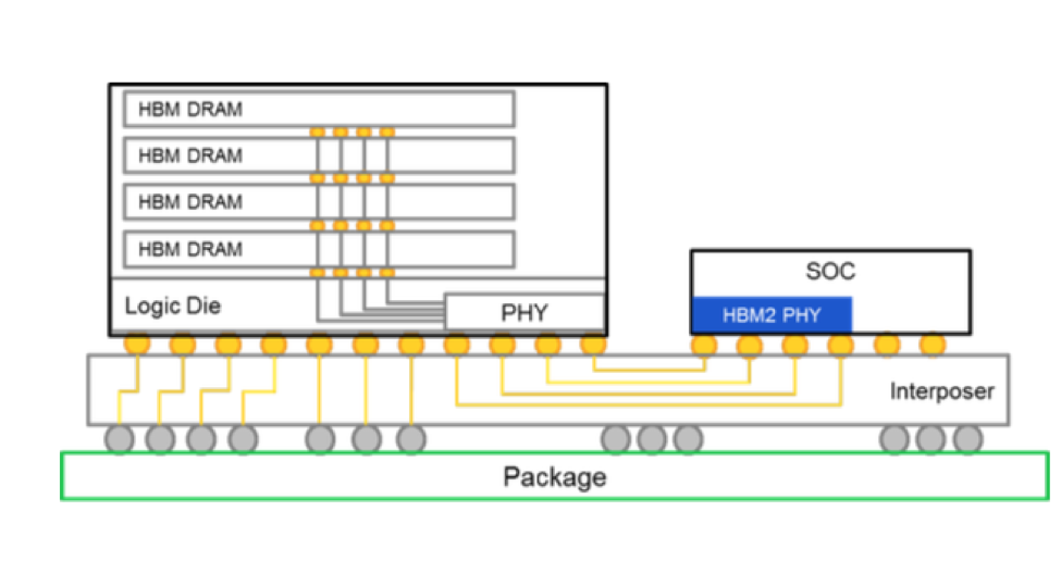
The HBM2 PHY – delivered as a fully characterized hard macro – includes all necessary components for robust operation, such as IO pads, PLL, clock distribution, transmit and receive paths, control logic, power distribution and electrostatic discharge (ESD) protection circuitry. Additional key HBM2 PHY product highlights include a DFI-style interface to the memory controller, 2.5D interposer connections between the PHY and DRAM, a validated memory controller interface, support for wafer-level and interposer testing, as well as availability with LabStation Validation Platform for enhanced bring-up and validation.
2.5D collaboration with GLOBALFOUNDRIES
In August, GLOBALFOUNDRIES demonstrated silicon functionality of a 2.5D packaging solution for its high-performance 14nm FinFET FX-14 integrated design system for application-specific integrated circuits (ASICs).
The 2.5D ASIC solution includes a stitched interposer capability to overcome lithography limitations and a two terabits per second (2Tbps) multi-lane HBM2 PHY, developed in partnership with Rambus. Building on the 14nm FinFET demonstration, the solution will be integrated on the company’s next-generation FX-7™ ASIC design system built on GF’s 7nm FinFET process technology.
As Dave Lammers of the GLOBALFOUNDRIES Foundry Files Blog recently noted, development of the PHY presented a “technical challenge” that Rambus engineers helped tackle along with the GF team.
“The HBM2 PHY is a mixed signal function that must be designed very specifically to each process node. [So], we [did extensive] modeling of the channel and then designed the PHY to meet those channel requirements,” Frank Ferro, senior director of product marketing at Rambus, told the Foundry Files. “[This] was a collaboration. We had long conference calls to [discuss] the whole process. But from day one, it worked, and that is a strong testament to the Rambus (modeling and signal integrity) tools and the engineers who have a history of designing these PHYs.”
According to Tad Wilder, a principal member of the technical staff at GLOBALFOUNDRIES, the two terabits-per-second of bandwidth is quite an impressive amount of bandwidth for a single core.
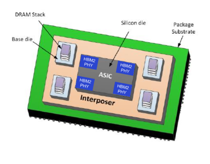
“With the ability to place up to four HBM2 PHYs on a chip, this gives ASIC designers an unprecedented eight terabits-per-second of low power, low latency DRAM access to work with,” he stated.
Wilder also confirmed that the 14nm HBM PHY “is the largest core we’ve produced for an ASIC,” with 15,000 internal pins talking to the memory controller and 1,700 external pins talking to the base die of the DRAM stack across the interposer.
28G Multi-protocol SerDes PHYs
In addition to showcasing our HBM2 PHY, we will be demoing our 28G Multi-protocol SerDes PHYs at the GLOBALFOUNDRIES Technology Conference.
Our 28G Multi-Protocol SerDes (MPS) PHYs support data rates from 1.25Gbps to 28.1Gbps across copper and backplane channels with more than 30dB insertion loss in a wide range of industry-standard interconnect protocols. They feature application-specific optimization enabled by an efficient and scalable architecture with adaptive and programmable receive equalization, as well as support for transmit FIR adaptation.
Additional key features include:
- Supports sharing of calibrated impedance codes among multiple PMAs to reduce the number of on- board reference resistors
- On-chip, AC-coupled receiver to eliminate on-board decoupling capacitors
- Adaptive receive equalizer with programmable settings providing up to 12dB of CTLE and 8-tap DFE
- Transmit FIR adaptation through back channel for Ethernet applications
- Supports Energy Efficient Ethernet
- x4-lane configurations with tight lane skew control
- BIST with PRBS generator
- In-situ real-time monitoring and receive data eye schmoo
- Optional LabStation for enhanced bring-up and validation
Interested in learning more? You can check out our HBM2 PHY product page here and our 28G SerDes PHY product page here.