Highlights:
- Built on a proven track record of over one hundred HBM design wins to ensure first-time silicon success
- Delivers up to 16 Gigabits per second per pin at low latency to meet the demands of next-generation AI and High-Performance Computing (HPC) workloads
- Expands industry-leading silicon IP portfolio of high-performance memory solutions
SAN JOSE, Calif. – March 4, 2026 – Rambus Inc. (NASDAQ: RMBS), a premier chip and silicon IP provider making data faster and safer, today announced the industry’s leading HBM4E Memory Controller IP, extending its market leadership in HBM IP. This new solution delivers breakthrough performance with advanced reliability features enabling designers to address the demanding memory bandwidth requirements of next-generation AI accelerators and graphics processing units (GPUs).
“Given the insatiable bandwidth demands of AI, it’s imperative for the memory ecosystem to continue aggressively advancing memory performance,” said Simon Blake-Wilson, SVP and general manager of Silicon IP, at Rambus. “As a leading silicon IP provider for AI applications, we are bringing the industry’s leading HBM4E Controller IP solution to the market as a key enabler for breakthrough performance in next-generation AI processors and accelerators.”
“HBM4E represents a significant milestone for HBM technology, delivering unprecedented performance for advanced AI and HPC workloads,” said Ben Rhew, corporate vice president and the head of the Foundry IP Development Team at Samsung Electronics. “HBM4E IP solutions will be essential for broad industry adoption, and Samsung looks forward to collaborating closely with Rambus and the wider ecosystem to drive innovation in AI.”
“HBM bandwidth is one of the main bottlenecks on LLM performance, and we’re excited by efforts across the industry to push it further,” said Reiner Pope, co-founder and CEO at MatX.
“AI processors and accelerators need high-performance, high-density HBM memory for the massive computational requirements of AI workloads,” said Soo Kyoum Kim, program associate vice president, Memory Semiconductors at IDC. “As the requirements of AI processors and accelerators continue their rapid rise, HBM solutions must advance apace. HBM4E IP reaching the market now will be an essential building block for designers of cutting-edge AI hardware.”
Rambus HBM4E Controller IP Features:
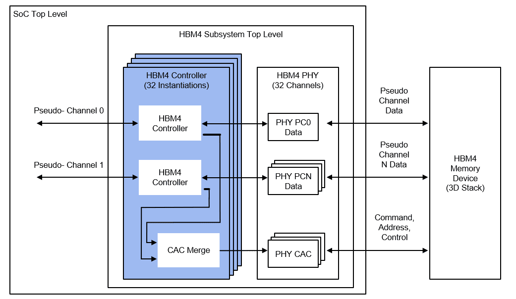
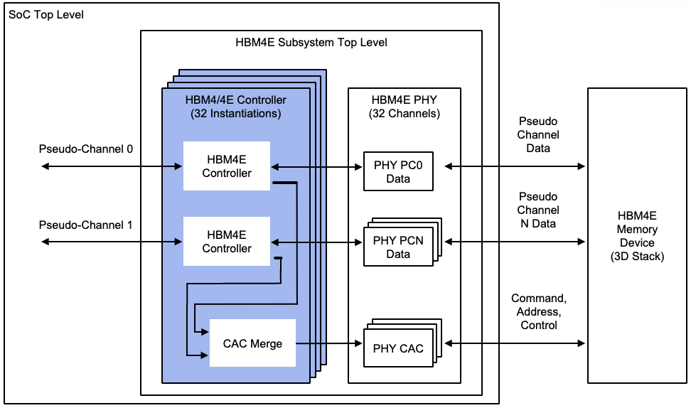
The Rambus HBM4E Controller enables a new generation of HBM memory deployments for cutting-edge AI accelerators, graphics and HPC applications. The HBM4E Controller is capable of supporting operation up to 16 Gigabits per second (Gbps) per pin providing an unprecedented throughput of 4.1 Terabytes per second (TB/s) to each memory device. For an AI accelerator with eight attached HBM4E devices, this translates to over 32 TB/s of memory bandwidth for next-generation AI workloads. The Rambus HBM4E Controller IP can be paired with third-party standard or TSV PHY solutions to instantiate a complete HBM4E memory subsystem in a 2.5D or 3D package as part of an AI SoC or custom base die solution.
Availability and More Information:
The Rambus HBM4E Controller IP is the latest addition to the Rambus leading-edge portfolio of digital controller solutions. The HBM4E Controller is available for licensing, and early access design customers can engage today.
Learn more about the Rambus HBM4E Controller IP at https://www.rambus.com/interface-ip/hbm/.
Forward-looking Statements
Information set forth in this press release, including statements as to Rambus’ outlook and financial estimates (if any) and statements as to the expected timing and effects of Rambus products, constitute forward-looking statements within the meaning of the safe harbor provisions of the Private Securities Litigation Reform Act of 1995.
These statements are based on various assumptions and the current expectations of the management of Rambus and may not be accurate because of risks and uncertainties surrounding these assumptions and expectations. Factors listed below, as well as other factors, may cause actual results to differ significantly from these forward-looking statements. There is no guarantee that any of the events anticipated by these forward-looking statements will occur, or what effect they will have on the operations or financial condition of Rambus. Forward-looking statements included herein are made as of the date hereof, and Rambus undertakes no obligation to publicly update or revise any forward-looking statement unless required to do so by federal securities laws.
Major risks, uncertainties and assumptions include, but are not limited to: any statements regarding anticipated operational and financial results; any statements of expectation or belief; other factors described under “Risk Factors” in Rambus’ Annual Report on Form 10-K and Quarterly Reports on Form 10-Q; and any statements of assumptions underlying any of the foregoing. It is not possible to predict or identify all such factors. Consequently, while the list of factors presented here is considered representative, no such list should be considered to be a complete statement of all potential risks and uncertainties.