Rambus’ silicon-proven, high-speed SerDes solutions
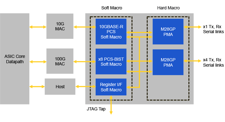
Rambus is now offering a suite of silicon-proven, high-speed SerDes solutions developed for the GLOBALFOUNDRIES high-performance FX-14™ ASIC platform. The suite includes 16G MPSL (multi-protocol serial link), 30G C2C (chip-to-chip) and 30G VSR (very short reach) PHYs.
Rambus’ SerDes PHYs include a physical media attachment (PMA) hard macro and physical coding sub-layer with a built-in self-test (PCS-BIST) soft macro. The PHYs can be configured to multiple channel widths and packaging options, thereby simplifying integration and maximizing design flexibility.

According to Luc Seraphin, senior vice president and general manager of the Rambus Memory and Interfaces Division, the Rambus SerDes PHYs are built on GLOBALFOUNDRIES 14nm FinFET (14LPP) process technology and optimized for power and area at peak bandwidth. This allows the PHYs to support Ethernet speeds up to 100Gb and beyond for high-speed wireline, wireless, 5G network infrastructure, high-performance servers, storage, connectivity and compute applications.
“Data traffic and bandwidth demands have exploded, driving the insatiable need for highly-optimized, high-performance semiconductor solutions,” Seraphin explained. “Through our collaboration with GLOBALFOUNDRIES, we are delivering robust high-speed interface IP that enables innovative chips and systems designed specifically for the data center and communications markets – helping GLOBALFOUNDRIES deliver value to its customers through tested solutions.”
GLOBALFOUNDRIES 14nm FinFET (14LPP) process technology
According to GLOBALFOUNDRIES, the FX-14 ASIC platform is a comprehensive semiconductor design system targeted for wired and wireless networking, storage and cloud computing applications. FX-14 is designed to deliver more performance per watt and use fewer watts per GHz in less space. Compared to its predecessor, FX-14 offers significant power and area savings, including:
- Up to 50% less active power
- Up to 85% less leakage
- Up to 55% less area
This combination of performance, power and area advantages can help chip designers stay ahead of system-level demands driven by evolving network and data center architectures and the race to 5G solutions.
Rambus HBM2 PHY: Developed for GLOBALFOUNDRIES FX-14 ASIC platform
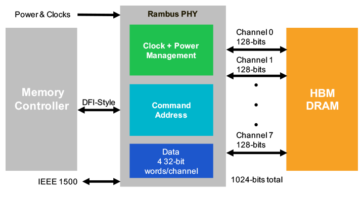
Earlier this year, Rambus announced the availability of its High Bandwidth Memory (HBM) Gen2 PHY, which was also developed for the GLOBALFOUNDRIES FX-14 ASIC Platform. Designed for systems that require low latency and high bandwidth memory, the Rambus HBM PHY, built on the GLOBALFOUNDRIES advanced 14nm Power Plus (LPP) process technology, targets networking and data center applications.

The PHY is fully compliant with the JEDEC HBM2 standard and supports data rates up to 2000 Mbps per data pin, enabling a total bandwidth of 256 Gigabytes per second. The Rambus HBM PHY delivers high performance with reduced power consumption when compared to other memory solutions. It combines 2.5D packaging with a wider interface (1024 bits) at a lower clock speed, which results in a higher overall throughput while remaining energy efficient for even the most high-performance computing applications. The Rambus HBM2 PHY is another key component in Rambus’ memory and SerDes high-speed interface IP portfolio for networking and data center applications.
