• Skip to primary navigation
  • Skip to main content
  • Skip to footer
  • English
  • Investor Relations
  • Resource Library
  • Newsroom
  • Blog
  • Careers
  • Support Center
Rambus Logo

Rambus

At Rambus, we create cutting-edge semiconductor and IP products, spanning memory and interfaces to security, smart sensors and lighting.

  • Products
      • All
          • Memory Interface Chips
          • DIMM Chipsets
          • DDR5 DIMM Chipset
          • DDR4 NVRCD
          • DDR4 Register Clock Driver
          • DDR4 Data Buffer
          • CXL Memory Interconnect Initiative
          • Interface IP
          • Memory PHYs
          • GDDR6 PHY
          • HBM3 PHY
          • HBM2E PHY
          • DDR4 PHY
          • More…
          • SerDes PHYs
          • PCIe 6.0 PHY
          • PCIe 5.0 PHY
          • 32G C2C PHY
          • 32G PHY
          • 28G PHY
          • More…
          • Digital Controllers
          • Memory Controllers
          • CXL & PCI Express Controllers
          • MIPI Controllers
          • Video Compression and Forward Error Correction Cores
          • Security IP
          • Root of Trust Solutions
          • Security Protocol Engines
          • Inline Cipher Engines
          • Crypto Accelerator Cores
          • DPA Countermeasures
          • Software Protocols & Crypto Toolkits
          • Anti-Counterfeiting
          • Provisioning and Key Management
      • Memory Interface Chips
        • DIMM Chipsets
          • DDR5 DIMM Chipset
          • Non-Volatile DDR4 Registering Clock Driver
          • DDR4 Register Clock Driver
          • DDR4 Data Buffer
          • DDR3 Register Clock Driver
          • DDR3 Isolation Memory Buffer
        • CXL Memory Interconnect Initiative

        • Made for high speed, reliability and power efficiency, our DDR3, DDR4, and DDR5 DIMM chipsets deliver top-of-the-line performance and capacity for the next wave of computing systems. Learn more about our Memory Interface Chip solutions
      • Interface IP
          • Memory PHYs
            • GDDR6 PHY
            • HBM3 PHY
            • HBM2E PHY
            • DDR4 PHY
            • DDR4 Multi-modal PHY
            • DDR3 PHY
          • SerDes PHYs
            • PCIe 6.0 PHY
            • PCIe 5.0 PHY
            • PCIe 4.0 PHY
            • 32G C2C PHY
            • 32G PHY
            • 28G PHY
            • 16G PHY
            • 12G PHY
            • 6G PHY
          • Digital Controllers
            • HBM3 Controller
            • HBM2E Controller
            • GDDR6 Controller
            • LPDDR5 Controller
            • CXL 2.0 Controller
            • PCIe 6.0 Controller
            • PCIe 5.0 Controller
            • MIPI CSI-2/DSI-2 Controllers
            • Video Compression and Forward Error Correction Cores
            • More…

        • With their reduced power consumption and industry-leading data rates, our line-up of memory interface IP solutions support a broad range of industry standards with improved margin and flexibility. Learn more about our Interface IP solutions
      • Security IP
          • Root of Trust Solutions
          • Security Protocol Engines
            • MACsec Engines
            • IPsec, TLS, SSL Multi-Protocol Engines
            • High Speed Public Key Accelerator
          • Inline Cipher Engines
          • Crypto Accelerator Cores
            • DPA Resistant Cores
            • Basic Crypto Blocks
          • Anti-Counterfeiting
            • CryptoFirewall Cores
            • Circuit Camouflage Technology
          • DPA Countermeasures
            • DPA Resistant Cores
            • DPA Resistant Software Libraries
            • DPA Workstation Platform
          • Software Protocols & Crypto Toolkits
            • IPsec Toolkit
            • FIPs Cryptographic Libraries
            • MACsec Toolkit
            • IoT Security Framework
          • CryptoMedia
            • Content Protection Core
            • Content Protection Services
          • Provisioning and Key Management
            • CryptoManager Provisioning
            • CryptoManager Device Key Management

        • From chip-to-cloud-to-crowd, Rambus secure silicon IP helps protect the world’s most valuable resource: data. Securing electronic systems at their hardware foundation, our embedded security solutions span areas including root of trust, tamper resistance, content protection and trusted provisioning. Learn more about our Security IP offerings
  • Markets
      • AI & Machine Learning
        • Speed and Security for the Artificial Intelligence & Machine Learning Revolution
          • Products
          • SerDes PHYs
          • Memory PHYs
          • Digital Controllers
          • Memory Interface Chips
          • Root of Trust
          • Crypto Accelerator Cores
          • Protocol Engines
          • Provisioning and Key Management
          • AI & Machine Learning
      • Automotive
        • Providing Performance & Security for the Connected Car
          • Products
          • Memory PHYs
          • SerDes PHYs
          • Digital Controllers
          • Root of Trust
          • PKE Engine
          • MACsec Engines
          • Crypto Accelerator Cores
          • Provisioning and Key Management
          • Explore Automotive
      • Data Center
        • Optimizing capacity, connectivity and capability of the cloud
          • Products
          • SerDes PHYs
          • Memory PHYs
          • Digital Controllers
          • Memory Interface Chips
          • Root of Trust
          • MACsec Engines
          • Software Protocols
          • Provisioning and Key Management
          • See Data Center
      • Edge
        • Catching a tidal wave of data
          • Products
          • Memory PHYs
          • SerDes PHYs
          • Digital Controllers
          • Root of Trust
          • Crypto Accelerator Cores
          • Protocol Engines
          • Software Protocols
          • Discover Edge
      • Government
        • Securing Mission-critical Systems
          • Products
          • Root of Trust
          • Protocol Engines
          • Anti-Tamper Cores
          • Provisioning and Key Management
          • DPA Workstation Platform
          • SerDes PHYs
          • Memory PHYs
          • Digital Controllers
          • See Government
      • IoT
        • Making IoT Data Safe & Fast
          • Products
          • Root of Trust
          • TLS Toolkits
          • Provisioning and Key Management
          • Memory PHYs
          • SerDes PHYs
          • Digital Controllers
          • Explore IoT
  • Resources
    • Inventions
    • Buying Guide
    • Resource Library
      • Webinars
      • Product Selector
  • About
      • Corporate Overview
      • Leadership
      • Inventors
      • Careers
      • Locations
      • Investor Relations
      • Newsroom
      • Blog
      • Events
      • Partnerships
      • Certifications
      • Corporate Responsibility
      • Contact
Home > Press Releases > Interface IP > Memory PHYs

Memory PHYs

Rambus Advances AI/ML Performance with 8.4 Gbps HBM3-Ready Memory Subsystem

Highlights: 

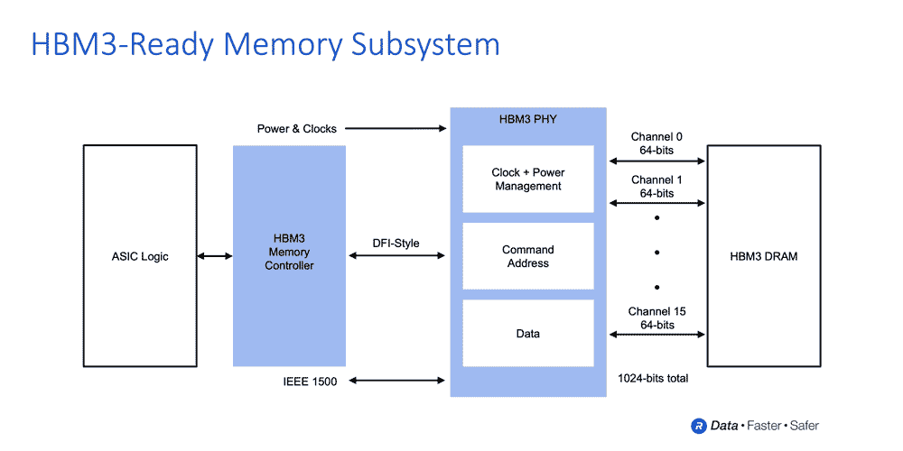
  • Provides HBM3-ready memory subsystem solution consisting of fully-integrated PHY and digital controller
  • Supports data rates up to 8.4 Gigabits per second (Gbps), enabling terabyte-scale bandwidth accelerators for artificial intelligence/machine learning (AI/ML) and high-performance computing (HPC) applications
  • Leverages market-leading HBM2/2E experience and installed-base to speed implementation of customer designs using next-generation HBM3 memory

HBM3 Ready Memory Subsytem

SAN JOSE, Calif. – Aug. 16, 2021 – Rambus Inc. (NASDAQ: RMBS), a premier chip and silicon IP provider making data faster and safer, today announced the Rambus HBM3-ready memory interface subsystem consisting of a fully-integrated PHY and digital controller. Supporting breakthrough data rates of up to 8.4 Gbps, the solution can deliver over a terabyte per second of bandwidth, more than double that of high-end HBM2E memory subsystems. With a market-leading position in HBM2/2E memory interface deployments, Rambus is ideally suited to enable customers’ implementations of accelerators using next-generation HBM3 memory.

“The memory bandwidth requirements of AI/ML training are insatiable with leading-edge training models now surpassing billions of parameters,” said Soo Kyoum Kim, associate vice president, Memory Semiconductors at IDC. “The Rambus HBM3-ready memory subsystem raises the bar for performance enabling state-of-the-art AI/ML and HPC applications.”

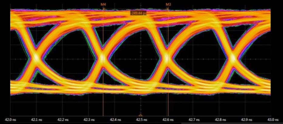
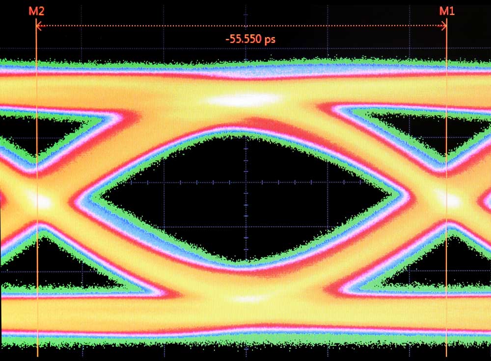
Rambus achieves HBM3 operation of up to 8.4 Gbps leveraging over 30 years of high-speed signaling expertise, and a strong history of 2.5D memory system architecture design and enablement. In addition to the fully-integrated HBM3-ready memory subsystem, Rambus provides its customers with interposer and package reference designs to speed their products to market.

“With the performance achieved by our HBM3-ready memory subsystem, designers can deliver the bandwidth needed by the most demanding designs,” said Matt Jones, general manager of Interface IP at Rambus. “Our fully-integrated PHY and digital controller solution builds on our broad installed base of HBM2 customer deployments and is backed by a full suite of support services to ensure first-time right implementations for mission-critical AI/ML designs.”

Benefits of the Rambus HBM3-ready Memory Interface Subsystem:

  • Supports up to 8.4 Gbps data rate delivering bandwidth of 1.075 Terabytes per second (TB/s)
  • Reduces ASIC design complexity and speeds time to market with fully-integrated PHY and digital controller
  • Delivers full bandwidth performance across all data traffic scenarios
  • Supports HBM3 RAS features
  • Includes built-in hardware-level performance activity monitor
  • Provides access to Rambus system and SI/PI experts helping ASIC designers to ensure maximum signal and power integrity for devices and systems
  • Includes 2.5D package and interposer reference design as part of IP license
  • Features LabStation™ development environment that enables quick system bring-up, characterization and debug
  • Enables the highest performance in applications including state-of-the-art AI/ML training and high-performance computing (HPC) systems

For more information on the Rambus Interface IP, including our PHYs and Controllers, please visit rambus.com/interface-ip.

Rambus Expands High-Performance Memory Subsystem Offerings with HBM2E Solution on Samsung 14/11nm

Highlights: 

  • Supports accelerators requiring terabyte-scale bandwidth for artificial intelligence/machine learning (AI/ML) training applications
  • Fully-integrated HBM2E memory interface subsystem, consisting of verified PHY and controller, silicon proven on advanced Samsung 14/11nm FinFET process
  • Backed by unrivaled system expertise supporting customers with interposer and package reference designs to speed time to market

SAN JOSE, Calif. – April 21, 2021 – Rambus Inc. (NASDAQ: RMBS), a provider of industry-leading chips and silicon IP making data faster and safer, today announced the Rambus HBM2E memory interface subsystem, consisting of a fully-integrated PHY and controller, is silicon proven on Samsung’s advanced 14/11nm FinFET process. Leveraging over 30 years of signal integrity expertise, the Rambus solution operates up to 3.2 Gbps, delivering 410 GB/s of bandwidth. This performance meets the terabyte-scale bandwidth needs of accelerators targeting the most demanding AI/ML training and high-performance computing (HPC) applications.

“Our partnership with Rambus brings together industry-leading memory interface design expertise with Samsung’s state-of-the-art process and packaging technologies,” said Jongshin Shin, vice president of Design Platform Development at Samsung Electronics. “Designers of AI and HPC systems can implement platforms using HBM2E memory leveraging Samsung’s advanced 14/11nm process to achieve unmatched levels of performance.”

The fully-integrated, production-ready Rambus HBM2E memory subsystem runs at 3.2 Gbps and provides designers with substantial headroom for implementation. Rambus and Samsung teamed to validate the HBM2E PHY and Memory Controller IP in silicon using Samsung’s 14/11nm process and advanced packaging technologies.

“With silicon operation up to 3.2 Gbps, customers can implement HBM2E memory subsystems with the confidence of ample margin for their designs,” said Matt Jones, general manager of IP Cores at Rambus. “Our customers benefit from our comprehensive support that includes 2.5D package and interposer reference designs, helping ensure first-time-right implementations.”

Benefits of the Rambus HBM2E Memory Interface (PHY and Controller):

  • Achieves speed of 3.2 Gbps per pin, delivering a system bandwidth of 410 GB/s from a single HBM2E DRAM 3D device.
  • Fully-integrated and verified in silicon HBM2E PHY and Controller reduces ASIC design complexity and speeds time to market
  • Includes 2.5D package and interposer reference design as part of IP license
  • Provides access to Rambus system and SI/PI experts helping ASIC designers to ensure maximum signal and power integrity for devices and systems
  • Features LabStation™ development environment that enables quick system bring-up, characterization and debug
  • Supports high-performance applications including state-of-the-art AI/ML training and high-performance computing (HPC) systems

For more information on the Rambus Interface IP, including our PHYs and Controllers, please visit rambus.com/interface-ip.

Rambus Advances HBM2E Performance to 4.0 Gbps for AI/ML Training Applications

Highlights: 

  • Fully-integrated HBM2E memory interface solution, consisting of verified PHY and controller, achieves industry’s fastest performance
  • New benchmark in performance supports accelerators requiring terabyte-scale bandwidth for artificial intelligence/machine learning (AI/ML) training applications
  • Partners with SK hynix and Alchip to develop 2.5D HBM2E memory system solution using TSMC N7 process and CoWoS® advanced packaging technologies
  • Offers unrivaled system expertise supporting customers with interposer and package reference designs to speed time to market

    Read first our primer on:
    HBM2E Implementation & Selection – The Ultimate Guide »

Figure 1 Rambus HBM2E Interface 4 Gbps Transmit Eye

SAN JOSE, Calif. – Sept. 9, 2020 – Rambus Inc. (NASDAQ: RMBS), a premier silicon IP and chip provider making data faster and safer, today announced it has achieved a record 4 Gbps performance with the Rambus HBM2E memory interface solution consisting of a fully-integrated PHY and controller. Paired with the industry’s fastest HBM2E DRAM from SK hynix operating at 3.6 Gbps, the solution can deliver 460 GB/s of bandwidth from a single HBM2E device. This performance meets the terabyte-scale bandwidth needs of accelerators targeting the most demanding AI/ML training and high-performance computing (HPC) applications.

“With this achievement by Rambus, designers of AI and HPC systems can now implement systems using the world’s fastest HBM2E DRAM running at 3.6 Gbps from SK hynix,” said Uksong Kang, vice president of product planning at SK hynix. “In July, we announced full-scale mass-production of HBM2E for state-of-the-art computing applications demanding the highest bandwidth available.”

The fully-integrated, production-ready Rambus HBM2E memory subsystem runs at 4 Gbps without PHY voltage overdrive. Rambus teamed with SK hynix and Alchip to implement the HBM2E 2.5D system to validate in silicon the Rambus HBM2E PHY and Memory Controller IP using TSMC’s N7 process and CoWoS® (Chip-on-Wafer-on-Substrate) advanced packaging technologies. Co-designing with the engineering team from Rambus, Alchip led the interposer and package substrate design.

“This advancement of Rambus and its partners, using TSMC’s advanced process and packaging technologies, is another important achievement of our ongoing collaboration with Rambus,” said Suk Lee, senior director of the Design Infrastructure Management Division at TSMC. “We look forward to a continued partnership with Rambus to enable the highest performance in AI/ML and HPC applications.”

“Alchip brought a demonstrated track record of success in 7nm and 2.5D package design to this initiative,” said Johnny Shen, CEO of Alchip Technologies. “We’re extremely proud of our contributions to Rambus’ breakthrough achievement.”

Rambus has 30 years of high-speed memory design applied to the most demanding computing applications. Its renowned signal integrity expertise was key to achieving an HBM2E memory interface capable of 4 Gbps operation. This raises a new benchmark for meeting the insatiable bandwidth requirements of AI/ML training.

“With silicon operation up to 4 Gbps, designers can future-proof their HBM2E implementations and can be confident of ample margin for 3.6 Gbps designs,” said Matthew Jones, senior director and general manager of IP cores at Rambus. “As part of every customer engagement, Rambus provides reference designs for the 2.5D package and interposer to ensure first-time right implementations for mission-critical AI/ML designs.”

Benefits of the Rambus HBM2E Memory Interface (PHY and Controller):

  • Achieves the industry’s highest speed of 4 Gbps per pin, delivering a system bandwidth of 460 GB from a single 3.6 Gbps HBM2E DRAM 3D device.
  • Fully-integrated and verified HBM2E PHY and Controller reduces ASIC design complexity and speeds time to market
  • Includes 2.5D package and interposer reference design as part of IP license
  • Provides access to Rambus system and SI/PI experts helping ASIC designers to ensure maximum signal and power integrity for devices and systems
  • Features LabStation™ development environment that enables quick system bring-up, characterization and debug
  • Supports high-performance applications including state-of-the-art AI/ML training and high-performance computing (HPC) systems

For more information on the Rambus Interface IP, including our PHYs and Controllers, please visit rambus.com/interface-ip.

Rambus Achieves Industry-Leading GDDR6 Performance at 18 Gbps

Highlights: 

  • Rambus GDDR6 Memory PHY has achieved the industry’s highest 18 Gbps performance
  • Leading-edge memory PHY IP is four-to-five times faster than current DDR4 solutions
  • Offers a complete and optimized memory subsystem of a GDDR6 PHY and a fully-integrated and verified memory controller
  • Rambus GDDR6 is well suited for artificial intelligence (AI), machine learning (ML), data center, networking and autonomous driving systems that need higher bandwidth memory

Rambus GDDR6 18 Gbps Transmit Eye

SUNNYVALE, Calif. – Oct. 30, 2019 –Rambus Inc. (NASDAQ: RMBS), a premier silicon IP and chip provider making data faster and safer, today announced it has achieved industry-leading 18 Gbps performance with the Rambus GDDR6 Memory PHY. Running at the industry’s fastest data rate of 18 Gbps, the Rambus GDDR6 PHY IP delivers peak performance four-to-five times faster than current DDR4 solutions and continues the company’s longstanding tradition of developing leading-edge products. The Rambus GDDR6 PHY pairs with the companion GDDR6 memory controller from the recent acquisition of Northwest Logic to provide a complete and optimized memory subsystem solution.

Increased data usage in applications such as AI, ML, data center, networking and automotive systems is driving a need for higher bandwidth memory. The coming introduction of high-bandwidth 5G networks will exacerbate this challenge. Working closely with our memory partners, the Rambus GDDR6 solution gives system designers more options in selecting the memory system that meets both their bandwidth and cost requirements.

“Memory bandwidth poses a significant obstacle for designers working on performance-intensive applications such as AI/ML,” said Hemant Dhulla, vice president and general manager of IP cores at Rambus. “With our GDDR6 18 Gbps memory subsystem, Rambus technology can unleash the power of leading-edge designs with a proven and cost-effective memory architecture.”

Benefits of the Rambus GDDR6 PHY:

  • Achieves the industry’s highest speed of up to 18 Gbps, delivering a maximum bandwidth of up to 72 GB/s
  • Complete and optimized memory subsystem solution with companion GDDR6 memory controller
  • Offers PCB and package design support – allowing customers to quickly and reliably bring their high-speed designs to production
  • Provides access to Rambus system and SI/PI experts helping ASIC designers to ensure maximized signal and power integrity for devices and systems
  • Features LabStation™ development environment that enables quick system bring-up, characterization and debug
  • Supports high-performance applications including networking, data center, ADAS, machine learning and AI

For more information on the Rambus Interface IP, including our PHYs and Controllers, please visit rambus.com/interface-ip.

Rambus Announces Portfolio of Advanced Memory and SerDes PHYs on TSMC N7 Process

Highlights:

  • GDDR6, HBM2, and 112G Long Reach (LR) interfaces designed for TSMC’s industry-leading N7 process technology expand Rambus’ leading-edge memory and SerDes PHY offerings
  • Portfolio enables critical building blocks for next-generation data center, networking, wireless 5G, high-performance computing (HPC), advanced driver assistance systems (ADAS), artificial intelligence (AI) and machine learning (ML) applications

SUNNYVALE, Calif. and SANTA CLARA, Calif. – Sep. 23, 2019 – Rambus Inc. (NASDAQ: RMBS), a premier silicon IP and chip provider making data faster and safer, today announced a broad portfolio of high-speed memory and SerDes PHYs for next-generation applications on TSMC’s industry-leading N7 process technology. Leveraging almost 30 years of high-speed interface design expertise and using leading process technology, Rambus offers GDDR6, HBM2 and 112G LR PHY IP available for licensing. These solutions enable demanding applications for data center, networking, wireless 5G, HPC, ADAS, AI and ML.

As the fastest discrete memory interface from Rambus, GDDR6 memory PHY adds to TSMC’s most comprehensive portfolio of silicon-proven intellectual property (IP), design tools and Reference Flows through the TSMC IP Alliance Program, a key component of TSMC Open Innovation Platform® (OIP). Along with HBM2 and 112G LR SerDes PHY, Rambus offers leading-edge memory and serial link interfaces for a broad range of high-performance applications.

“TSMC OIP Alliance partners continue to deliver innovative solutions that will address the tremendous demands for computing power driven by AI and next-generation networks,” said Suk Lee, TSMC senior director, Design Infrastructure Management Division. “We’re pleased with the availability of Rambus’ high-speed memory and SerDes interface solutions on TSMC’s industry-leading N7 process technology to address customer’s requirements for the most demanding applications.”

Expanding beyond the traditional GPU and graphics applications, GDDR6 and HBM2 address market needs in multiple, advanced applications like AI/ML, ADAS and networking, as memory bandwidth becomes more critical for overall system performance. As the industry rapidly transitions to 400 and 800GbE communications systems, 112G LR is a key building block necessary to support the ever-growing demand for more bandwidth in data center and network applications.

“This announcement highlights Rambus’ leadership in high-speed SerDes and memory PHY IP, leveraging the company’s long tradition of signal- and power-integrity expertise,” said Hemant Dhulla, vice president and general manager of IP cores at Rambus. “We are very proud to be able to offer these advanced solutions as part of the TSMC ecosystem.”

Availability
The Rambus GDDR6 and HBM2 Memory PHYs, and 112G LR SerDes PHY are available from Rambus today for licensing and integrating into system-on-chip (SoC) designs.

Demonstration Details at TSMC 2019 Open Innovation Platform® Ecosystem Forum
Join Rambus in Booth #408 at the TSMC 2019 Open Innovation Platform® Ecosystem Forum on September 26, 2019 at the Santa Clara Convention Center in Santa Clara, California and learn more about its extensive portfolio of interface IP and innovation in advanced memory and interface technology.

Additional Information
To learn more about the TSMC 2019 Open Innovation Platform® Ecosystem Forum, visit https://www.rambus.com/event/tsmc-oip-santa-clara-2019/. For additional details about Rambus silicon applications or more information on our latest Rambus high-speed memory and SerDes PHY solutions, go to rambus.com/interface-ip/.

Rambus to Acquire Northwest Logic, Extending Leadership in Interface IP

Highlights:

  • Complementary product portfolio of PHYs and controllers further accelerates Rambus growth
  • Expands solutions for data center, artificial intelligence (AI), machine learning (ML), communications and automotive applications
  • Combined offerings, including HBM2, GDDR6, DDR4 and PCI Express (PCIe), create one-stop-shop for SoC designers

SUNNYVALE, Calif. and HILLSBORO, Ore. – July 29, 2019 – Rambus Inc. (NASDAQ: RMBS), a premier silicon IP and chip provider making data faster and safer, today announced it has signed a definitive agreement to acquire Northwest Logic, a market leader in memory, PCIe and MIPI digital controllers. Northwest Logic’s high-performance, high-quality and silicon-proven digital IP controller cores are optimized for use in both ASICs and FPGAs. Interface IP solutions consisting of a physical interface (PHY) and companion digital controller make it possible to optimize the transfer of data between chips and electronic devices. Every SoC design that uses a Memory or a PCIe or a MIPI PHY also needs to use a controller associated with it. The combination of complementary digital and physical IP portfolios from Northwest Logic and Rambus will create a one-stop-shop for customers.

“With this acquisition, we expand our leading product portfolio for high-performance markets such as data center, networking, artificial intelligence, machine learning and automotive,” said Hemant Dhulla, vice president and general manager of IP Cores at Rambus. “Northwest Logic’s innovative, best-in-class digital controllers complement Rambus’ proven strength in high-speed physical IP cores. Together, we will offer one of the most comprehensive high-performance interface IP solutions in the industry, leveraging our core strength in semiconductors, strong go-to-market advantage and global reach.”

Brian Daellenbach, president and CEO, Northwest Logic said: “Northwest Logic’s category-leading digital controllers fit perfectly with Rambus’ leadership portfolio of high-speed PHY solutions. This deal creates a one-stop-shop for SoC designers working on state-of-the-art applications across a broad range of high-performance markets. We look forward to continue serving our existing customers and working with our PHY partners.”

Critical to enabling the high performance of data center, networking, AI, ML and automotive applications, this acquisition will bring together the physical and digital IP core families from renowned market leaders to offer comprehensive memory and SerDes IP solutions for chip designers.

The transaction is expected to close in the current calendar quarter of 2019. Although this transaction will not materially impact 2019 results due to the expected timing of close and acquisition accounting, Rambus expects this acquisition to be accretive in 2020.

Forward-looking statements
Information set forth in this press release, including statements as to Rambus’ outlook and financial estimates and statements as to the expected timing, completion and effects of the proposed acquisition of Northwest Logic, constitute forward-looking statements within the meaning of the safe harbor provisions of the Private Securities Litigation Reform Act of 1995.

These statements are based on various assumptions and the current expectations of the management of Rambus and may not be accurate because of risks and uncertainties surrounding these assumptions and expectations. Factors listed below, as well as other factors, may cause actual results to differ significantly from these forward-looking statements. There is no guarantee that any of the events anticipated by these forward-looking statements will occur, or what effect they will have on the operations or financial condition of Rambus or Northwest Logic. Forward-looking statements included herein are made as of the date hereof, and Rambus undertakes no obligation to publicly update or revise any forward-looking statement unless required to do so by federal securities laws.

Major risks, uncertainties and assumptions include, but are not limited to: the expected benefits and costs of the transaction; management plans relating to the transaction; the expected timing of the completion of the transaction; the satisfaction of all closing conditions to the transaction; statements of the plans, strategies and objectives of Rambus for future operations; any statements regarding anticipated operational and financial results; any statements of expectation or belief; the risk that disruptions from the transaction will harm Rambus’ business; other factors described under “Risk Factors” in Rambus’ Annual Report on Form 10-K and Quarterly Reports on Form 10-Q; and any statements of assumptions underlying any of the foregoing.  It is not possible to predict or identify all such factors. Consequently, while the list of factors presented here is considered representative, no such list should be considered to be a complete statement of all potential risks and uncertainties.

  • Go to page 1
  • Go to page 2
  • Go to page 3
  • Interim pages omitted …
  • Go to page 6
  • Go to Next Page »

Footer

About

  • Corporate Overview
  • Leadership
  • Careers
  • Locations
  • Investor Relations
  • News
  • Corporate Responsibility

Products

  • Memory PHYs
  • SerDes PHYs
  • Digital Controllers
  • Server DIMM Chipsets
  • Root of Trust Solutions
  • Provisioning and Key Management
  • Protocol Engines
  • Crypto Accelerator Cores
  • Software Protocols
  • DPA Countermeasures
  • Anti-Counterfeiting
  • CryptoMedia

Markets

  • AI & Machine Learning
  • Automotive
  • Data Center
  • Edge
  • Government
  • IoT
  • Pay TV

Resources

  • Resource Library
  • Webinars
  • Inventions
  • Buying Guide
  • Contact

Copyright © 2023 Rambus.com. All Rights Reserved. Privacy Policy | Trademark & Guidelines

  • Facebook icon
  • Twitter icon
  • YouTuve icon
  • LinkedIn icon
  • Blog icon